We are pleased to inform you that MetroSemi offers customized GaN epitaxial wafers. Our GaN epitaxial wafers are specifically tailored to meet your unique requirements and specifications.
Features Overview
Typical Applications
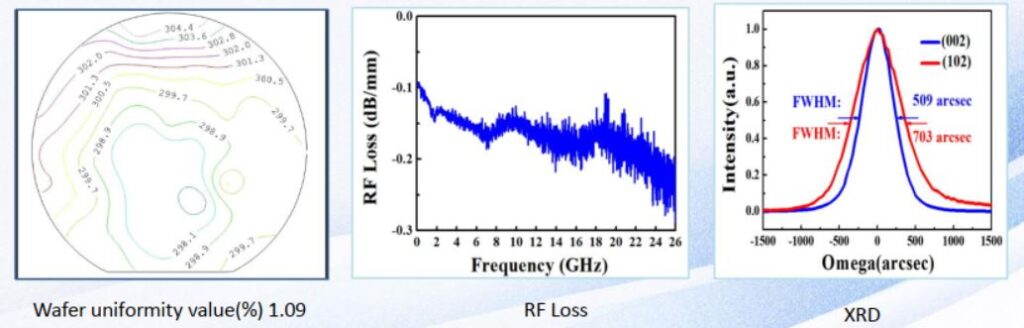
High uniformity and good repeatability
Low RF loss
“4”, and “6” available
5G and 6G wireless communications
Solid-state RF energy application
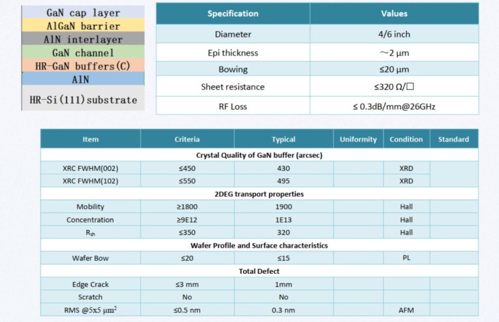
Wafer Size and Epi-Structure
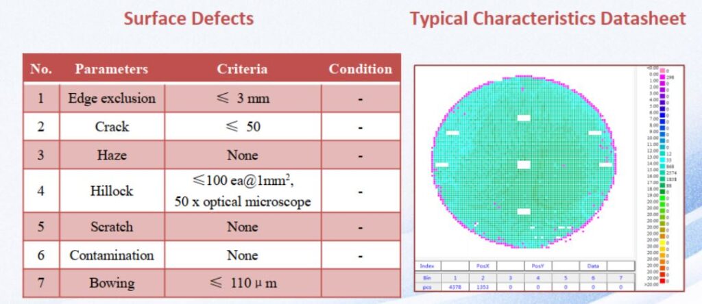
Typical Characteristics Datasheet
Features Overview
Typical Applications
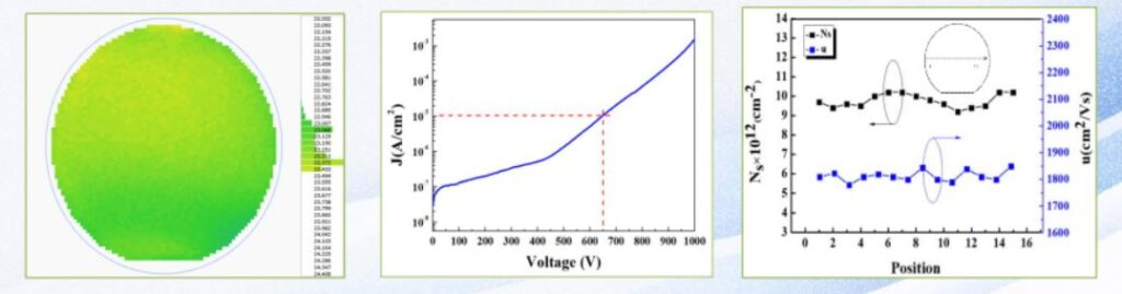
High uniformity and good repeatability
Low leakage current with excellent 2DEG transport properties
Breakdown voltage ≥ 650 V
4”, 6” and 8” available
RoHS compliant
Suitable for power HEMTs and low cost CMOS process,
Suitable for power diodes
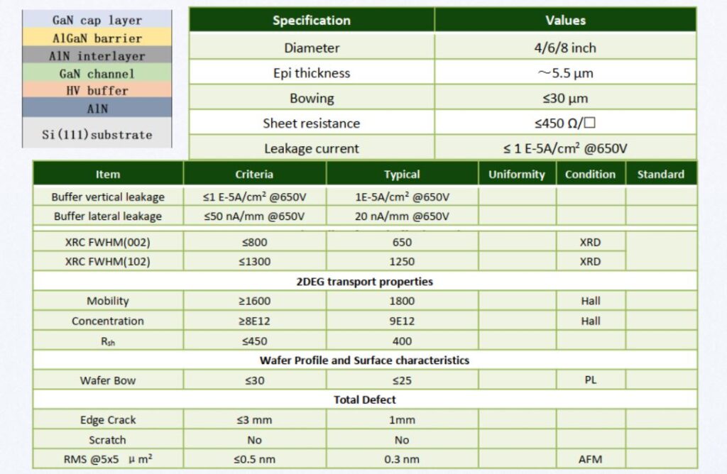
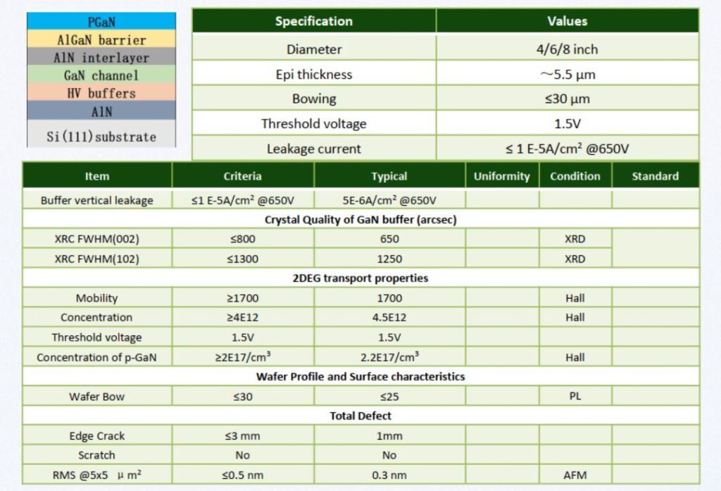
Wafer Size and Epi-Structure
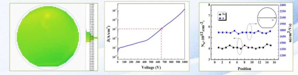
Typical Characteristics Datasheet
Features Overview
Typical Applications
High uniformity and good repeatability
Low leakage current with excellent 2DEG transport properties
Breakdown voltage ≥ 650 V
4”, 6” and 8” available
RoHS compliant
P-GaN
Suitable for power E-mode HEMTs and low cost CMOS process,
Suitable for power diodes
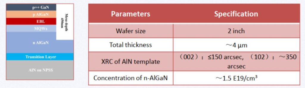
Wafer Size and Epi-Structure
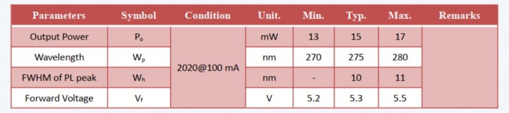
Typical Characteristics Datasheet
Features Overview High uniformity and good repeatability Based on NPSS or AlN template