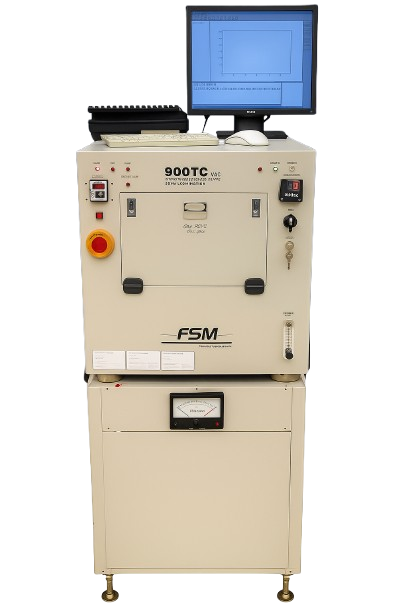
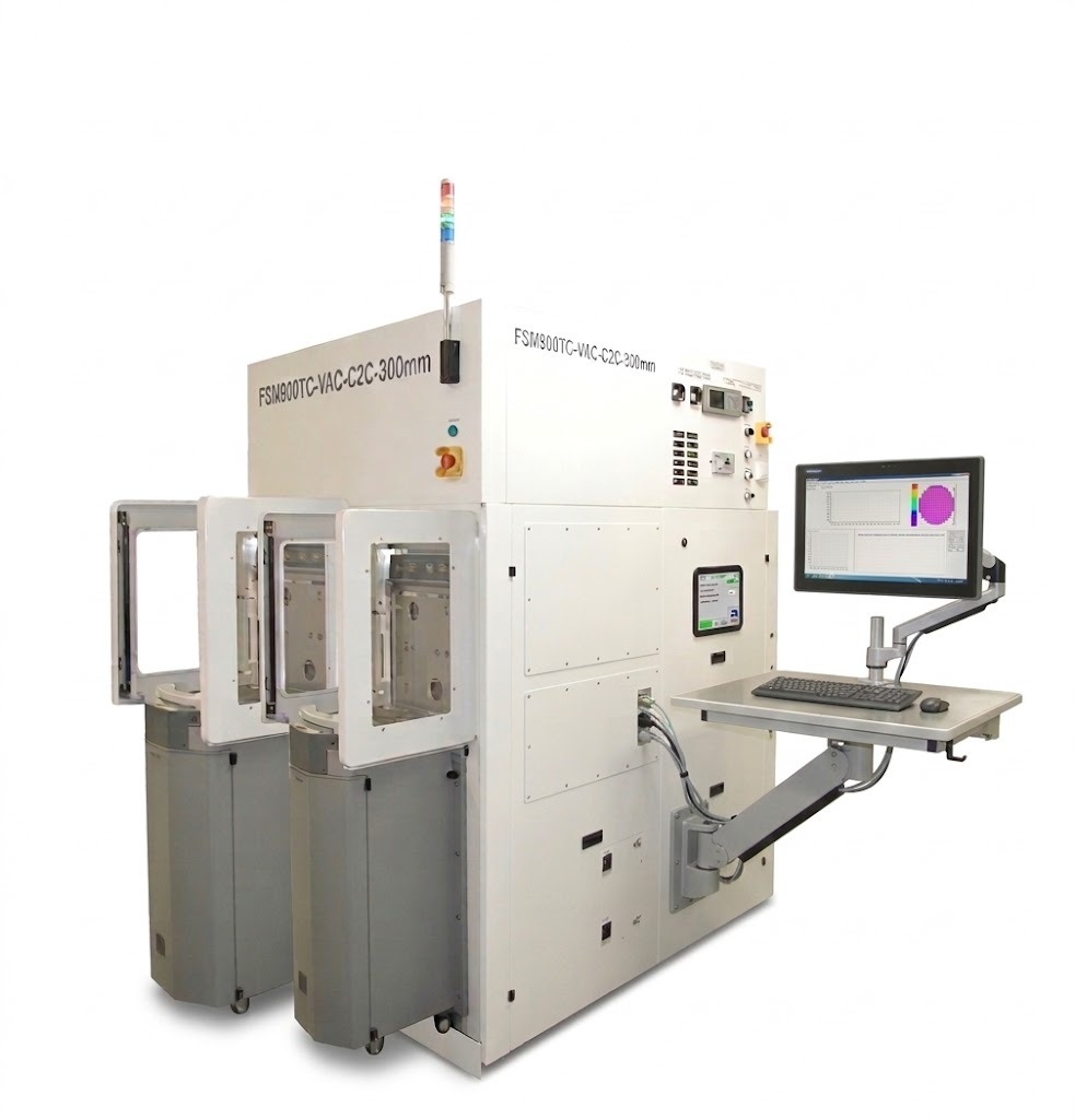
FSM 900TC-Vac, High-Temperature Wafer Stress & Bow Measurement System
Comprehensive Thermal Mechanical Characterization
Introduction
The FSM 900TC-Vac is a state-of-the-art system for wafer stress and bow height measurement at elevated temperatures. Utilizing a non-contact laser triangulation technique and a vacuum chamber capable of reaching 900°C, it supports wafers 50mm to 200mm/300mm. Designed for semiconductor, MEMS, solar, LED, and FPD applications, it features integrated Thermal Desorption Spectroscopy (TDS) for advanced metrology.
Key Features
Stress & Bow Measurement: Reliable performance at high temperatures.
Thermal Cycle Capability: Programmable for inert gas (up to 900°C) or vacuum (up to 1100°C).
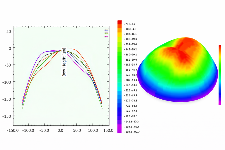
Wide Bow Range: Measures bow from sub-micron to millimeter scales.
Advanced Optics: Dual laser system adapts to reflective and translucent films.
Whole Wafer Monitoring: Trend analysis with up to 100 channels.
Software & Export: Windows compatibility, JPEG exports, and CTE calculation.
Technical Specifications
Temperature Range: Room temperature to 900°C (optional 1100°C).
Ramp Rate: 1–50°C/min, programmable with ramp and hold cycles.
Wafer Size: 50mm to 300mm (round or square).
Vacuum: Turbo molecular dry pump, up to 5×10⁻⁶ Torr.
Inert Gas Options: Nitrogen, Argon, Forming Gas.
Chamber Design: RTP-type with tungsten halogen lamps, gold-plated reflective walls, and water cooling.
Sample Loading: Quartz susceptor for smooth operation.
Footprint: Main Unit: 26” (W) X 58.24” (D)
Accessory Cart (Resistivity): 20” (W) X 20” (D)
Weight: 400 lbs.
Power: 208V, 30A, 3-phase, 5 wires (neutral and ground).
Optional Capabilities
Film Thickness Measurement: Accurate for films ≥3000Å at up to 600°C.
Reflectivity Measurement: Spectrometer-based, with adjustable wavelengths up to 600°C.
Sheet Resistivity: 4-point probe measurement up to 400°C.
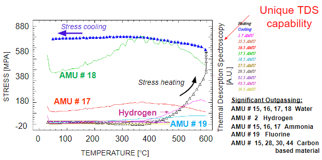
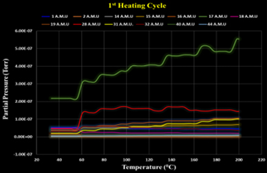
Thermal Desorption Spectrometry (TDS): Quadruple mass spectrometer for outgassing analysis during heating.
FSM900TC
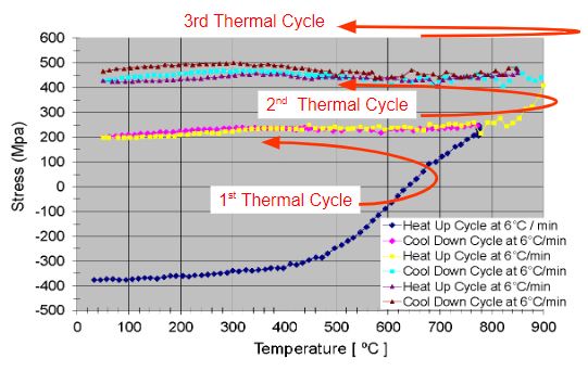
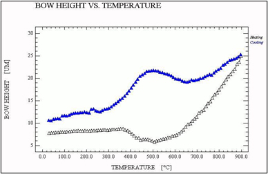
FSM 900TC-Vac Integrated Metrology Annealing Chamber By incorporating multiple probes, the FSM 900TC-Vac allows for the simultaneous extraction of stress hysteresis, thermal desorption spectroscopy (TDS), film shrinkage, resistivity, and reflectivity changes in the film.
CONFIGURATION
Film Stress
Standard
Vacuum Annealing Oven
Standard
Thermal Desorption
Standard
Film Thickness
Option
Reflectivity
Option
Sheet Resistance
Option
Temperature Range, 900°C
Standard
2D/3D Stress Mapping
Option
FSM 900TC-C2C
FSM900TC C2C
FSM 900TC-Vac Integrated Metrology Chamber
(200mm or 300mm Water Option)
Rapid Thermal Mechanical Characterization of Low K Dielectrics, Copper & other Thin Films for Semiconductor, MEMS, Solar, LED, and FPD Applications (upto 900°C)
Why Vacuum Annealing Chamber?
With the drive towards smaller line width and higher speed devices, process integration will involve new thin film materials like low K, copper and other novel materials. However, several of these new materials are very sensitive to oxidation at elevated temperatures. They are also prone to outgas, or exhibit physical and material changes upon heating.To help characterize these changes, the FSM-900TC-Vac offers sealed heating type chamber that simulates process conditions. It can operate either under a completely inert gas environment (with a very low partial pressure of oxygen) or under high vacuum mode.
Why integrated metrology?
By incorporating multiple probes around this chamber . Stress hysteresis, thermal desorption, film shrinkage and reflectivity changes in the thin film can be simultaneously extracted. This approach overcomes sample to sample and tool variations for new material characterization. By integrating these metrology data, FSM-900TC-Vac can quickly profile the thermal stability and thermal loading capacity for new materials. For example, the type of material outgassing at specific temperature can be correlated or overlaid graphically with data from film thickness/shrinkage, reflectivity and stress hysteresis profiles. Probes are also available to study resistivity changes from monitoring grain growth or phase changes. This novel integrated metrology approach can dramatically speed up new material screening and help compress the process integration cycle at the various technology nodes.