
InSight AFP — Automated Atomic Force Profiler for Semiconductor Metrology
Introduction
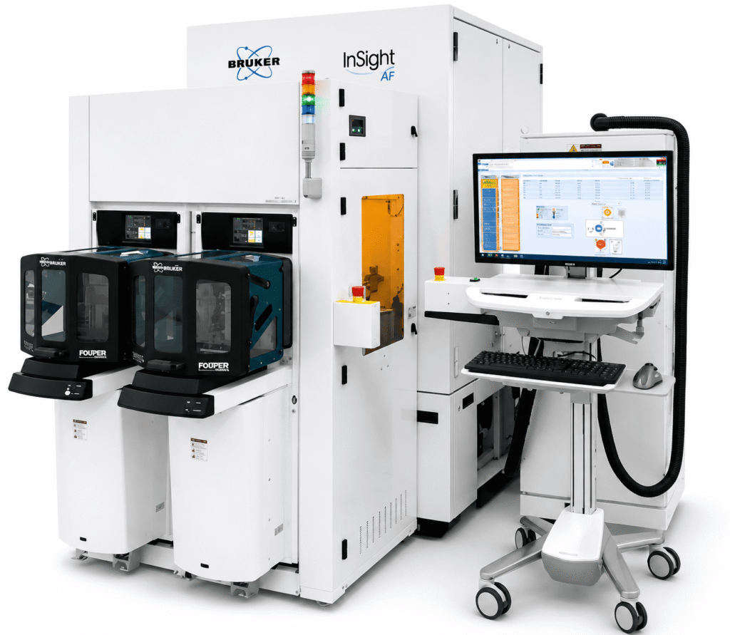
The InSight AFP is Bruker’s fifth-generation automated atomic force profiler (AFP), offering the industry’s highest resolution, fastest profiling, and rapid 3D die mapping. It is positioned as the world’s highest-performance, industry-preferred CMP profiling and etch-depth metrology system for advanced technology nodes. Its modern tip scanner, combined with inherently stable capacitive gauges and an accurate air-bearing positioning system, enables non-destructive, direct measurement in the active area of dies — eliminating dependence on test keys or destructive cross-sectioning for many measurement tasks.
Key Features
- TrueSense® technology delivering the proven long-scan capability of an atomic force profiler with the industry’s highest resolution and longest tip life
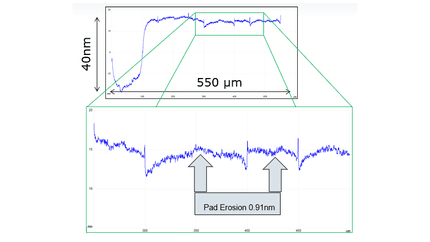
- Fully automated etch-depth, dishing, and erosion monitoring on submicron features with unsurpassed repeatability, without relying on test keys or models
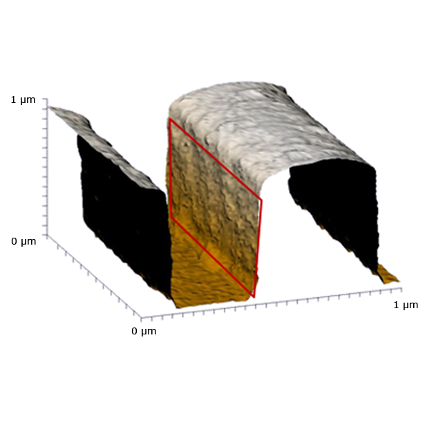
- Proprietary CDMode for characterizing sidewall features and roughness, reducing the amount of required cross-sectioning and providing direct sidewall roughness data unobtainable through other techniques
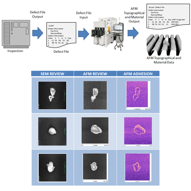
- Automated defect review and classification, delivering fast, actionable topographical and material information on wafer and photomask defects for high-volume manufacturing (HVM)
- 100x high-resolution registration optics with AFM Global Alignment for less than ±250nm raw image placement accuracy on patterned wafers and masks
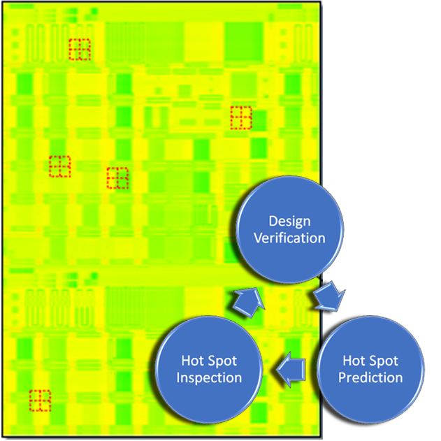
- 3D die mapping with HyperMap™, enabling full reticle-field scans with automated hot-spot detection and review
- Full compatibility with KLARITY and most other yield-management systems (YMS)
Operating Principle
The InSight AFP operates as an automated atomic force profiler: a tip-scanning head with capacitive position sensing and air-bearing stage positioning traces the surface topography of a sample in a closed-loop, force-feedback manner, generating direct, non-destructive 3D measurements within the active die area rather than relying on modeled or test-key proxies. Two proprietary adaptive modes extend this core principle: DTMode, an adaptive scan mode proven to deliver the lowest Total Measurement Uncertainty (TMU) of any AFM for depth metrology, and TrueSense™ mode, which relies on instantaneous feedback enabling picoNewton force control for the highest-accuracy, non-destructive surface profiling.
Measurement Capabilities
- CMP post-polish residual topography detection with picometer sensitivity
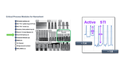
- Etch depth, dishing, and erosion measurement on submicron features
- Sidewall feature and roughness characterization (CDMode)
- Top Line Roughness (LTR) measurement for EUV lithography process monitoring
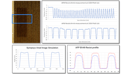
- Resist profile shrinkage characterization for EUV process development
- Automated defect topography and classification review
Technical Specifications
Parameter | Value |
Long-term stability | 0.3nm — NIST-traceable reference metrology with stability measured over one year |
Inline throughput | 260–340 sites/hour, with reduced move-acquire-measure (MAM) times supporting up to 50 wafers/hour |
Profiling speed | Up to 36,000µm/sec |
Scan range | 105µm extended-range, super-flat scanner |
Out-of-plane motion | Less than 1nm over the entire 105µm scan range |
Probe-to-probe repeatability | 2 picometer, long-term repeatability and reproducibility |
Depth metrology MAM time | Less than 10 seconds (via DTMode) |
Image placement accuracy | Less than ±250nm raw placement accuracy (patterned wafer/mask) |
Reticle field scan example | Full 26mm × 33mm reticle field acquired in 24 hours at 1µm × 1µm pixel size |
Hot-spot inspection scan rate | 26mm/sec across 33,000 scan lines (example dataset) |
Scanning Modes
- CDMode — sidewall feature and roughness characterization
- DTMode — proprietary adaptive scan mode optimized for lowest-TMU depth metrology
- TrueSense™ mode — picoNewton force-controlled, non-destructive high-resolution profiling
- Large Area Scanning mode — extends metrology coverage from tens of nanometers up to full 300mm wafer scale
- Hot Spot Detection and Review — automated rescanning of flagged defect/hot-spot locations
Sample Size & Wafer Handling
- Full-die and full-reticle-field coverage, including 33mm × 26mm flash fields and larger
- Metrology coverage scaling from tens of nanometers up to full 300mm wafers (via Large Area Scanning combined with the 105µm scanner)
- Optimized wafer handling supporting throughput up to 50 wafers/hour
Automation Features
- Fully automated, inline process control for etch and CMP wafers
- Automated hot-spot detection and review after high-speed die/reticle mapping
- AFM Global Alignment for automated, high-accuracy defect-of-interest targeting
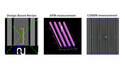
- Recipe writing via an XML/CAD interface in under 5 minutes, supporting fast process-development turnaround
- Shared recipes between AFP and SEM systems via the XML interface for correlated, co-located measurement
Software Capabilities
- Simple, intuitive recipe interface for metrology through an XML/CAD interface
- HyperMap™ software for 3D die mapping and hot-spot visualization
- Full compatibility with KLARITY and most other yield-management systems
- Defect classification workflows supporting rapid HVM defectivity source identification
Environmental Control & Stability
- Air-bearing positioning system for high-precision, stable stage motion
- Inherently stable capacitive gauges supporting long-term (one-year measured) 0.3nm stability
- NIST-traceable reference metrology for process-control-grade data trust
Semiconductor Applications
- Wafer surface roughness measurement: sub-nanometer topography sensitivity across front, mid, back, and far-back end-of-line process steps
- CMP process monitoring: CMP Advanced Process Control with picometer sensitivity to detect post-polish residual topography and 2-picometer long-term repeatability
- Defect inspection: automated defect review and classification for rapid identification of device-killing defects on wafers and photomasks
- Critical dimension (CD) metrology: CDMode sidewall and roughness characterization, reducing reliance on destructive cross-sectioning
- Thin-film / etch characterization: DTMode etch-depth metrology with sub-10-second MAM time and the lowest published Total Measurement Uncertainty for depth metrology
- Advanced packaging / process development: recipe-driven metrology enabling short-loop, complex DOE process development for logic and memory nodes
- Lithography / EUV process control: Top Line Roughness (LTR) monitoring, shown to correlate with defectivity and yield outcomes across resist formulations
- Failure analysis / co-located metrology: non-destructive hybrid metrology sharing exact measurement locations between AFP and SEM via shared recipes and sub-250nm placement accuracy
Advantages for Semiconductor Manufacturing & Research
- Accuracy & sensitivity: picometer-level sensitivity for post-polish residual topography and sub-nanometer out-of-plane scanner motion across the full 105µm range
- Repeatability: 2 picometer long-term probe-to-probe repeatability and reproducibility, with NIST-traceable one-year stability of 0.3nm
- Throughput: 260–340 sites/hour inline throughput, up to 50 wafers/hour, and profiling speeds up to 36,000µm/sec
- Ease of operation: recipe writing in under 5 minutes via an intuitive XML/CAD interface, plus automated hot-spot detection/review that reduces manual operator intervention
Industries / Users Served
Advanced logic and memory manufacturers, foundries running CMP and etch process control, EUV lithography process-development teams, and photomask/HVM defect-review operations — applications explicitly named by Bruker include CMP Advanced Process Control, Etch Advanced Process Control, Etch Process Development, CMP Process Development, Lithography EUV APC, and Lithography EUV Process Development.