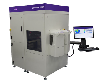
The Candela® 8720 advanced surface inspection system captures a variety of mission-critical substrate and epitaxial defects for the LED, photonics, communications and other compound semiconductor markets. Implementation of automated wafer inspection with statistical process control (SPC) methodology can significantly cut yield loss due to epi defects, minimize metal-organic chemical vapor deposition (MOCVD) reactor process excursions, and increase MOCVD reactor uptime.
Automated defect inspection for LED materials, enabling enhanced quality control of substrates, fast time-to-root cause determination, and improved MOCVD process control
A single-tool solution that combines multiple optical inspection techniques in a single scan for maximum efficiency in automated defect detection and classification
High sensitivity to yield-impacting defects across multiple compound semiconductor substrates
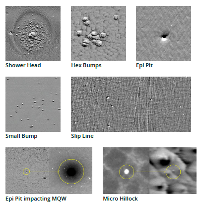
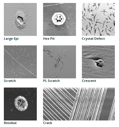
The Candela 8720 system can be operated in three modes to meet the needs of various applications: high-throughput, standard resolution, and high resolution. In the high-throughput mode, the Candela 8720 system can be used as a simple particle counter for process tool monitoring and qualification applications. In the advanced classification / high-sensitivity mode, multiple detection channels enable accurate detection and classification of various defect types to characterize process-related issues and identify yield-impacting defects. The inspection method achieves full-surface coverage in minutes to produce high-resolution images and wafer maps with automatically classified defects.