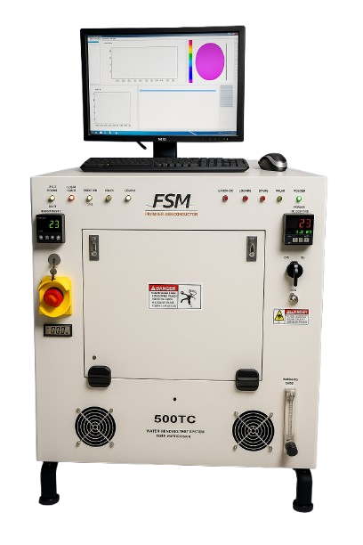
FSM 500TC High-Temperature Bow & Stress Measurement System
Characterizing Thermal Properties & Stability of Thin Film Materials
Introduction
The FSM 500TC High-Temperature Measurement System is designed for researchers and process engineers to evaluate the thermal properties and stability of thin films in semiconductor, III-V, optoelectronics, and MEMS materials subjected to thermal cycles. This critical tool aids in identifying issues such as film cracking, voiding, and hillock formation—common challenges that can lead to reliability concerns in manufacturing. By using FSM 500TC, you can assess the maturity of new processes and materials before production deployment. The FSM 500TC’s intuitive user interface ensures ease of operation for both dedicated operators and occasional users, whether in R&D or production environments.
Key Features
- Versatility
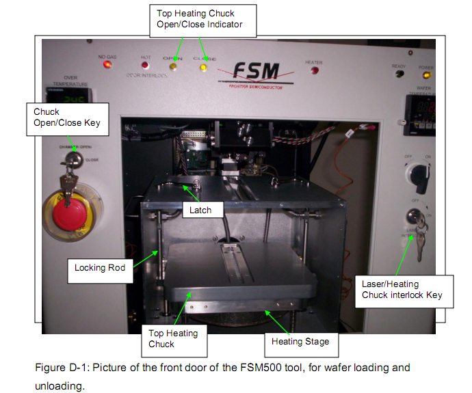
Accommodates 50mm to 200mm/300mm wafers without changing sample holders or jigs. Performs stress and wafer bow measurements at both room and high temperatures. - Simple Sample Handling
Convenient wafer placement on the heat chuck stage with location pins ensures consistent, reproducible operation. - Auto Switching Dual Laser
Patented dual-laser technology automatically switches wavelengths (650nm and 780nm) based on sample reflectivity, enabling measurements on diverse films, including nitrides, polyimides, low-k, high-k materials, and metals. - Programmable Temperature Cycling
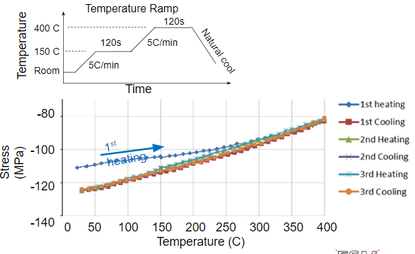
Create recipes for single or multiple heat cycles with programmable ramp rates and annealing temperatures to evaluate thermal stability. - Data Management & Reporting
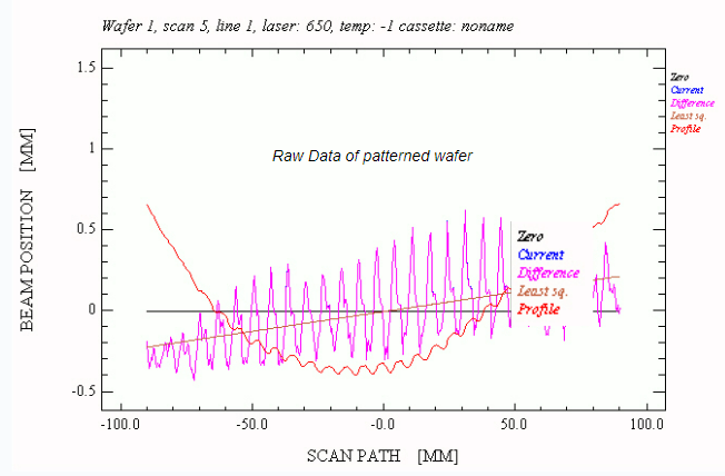
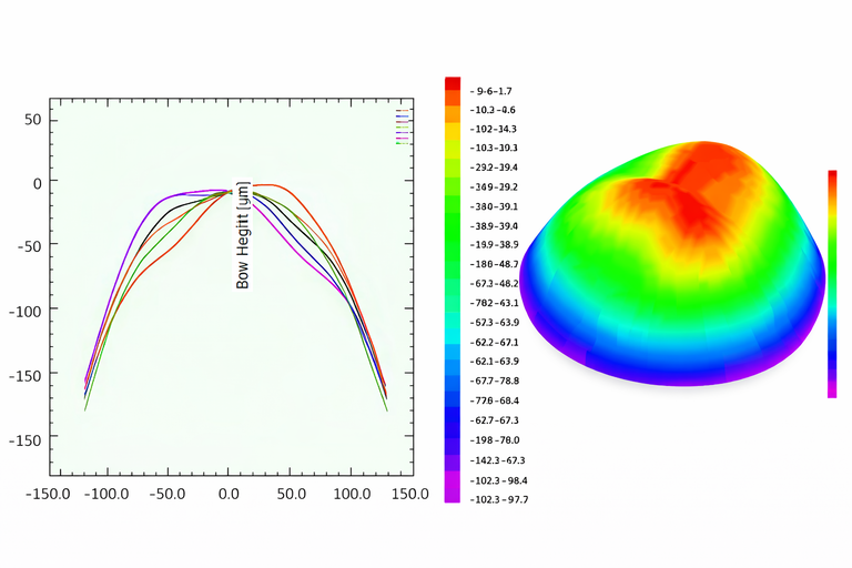
Exportable graphs and results—such as Stress vs. Temperature, Stress vs. Time, or Wafer Bow vs. Temperature—facilitate report generation in Excel™ or Word. Standard features include Coefficient of Thermal Expansion calculations.
Specifications
- Operating Temperature: Ambient to 500°C
- Heating Method: Resistive heat chuck with air cooling
- Measurement Technique: Non-contact laser scanning
- Wafer Size: 50mm to 200mm/300mm (round or square)
- Scanning Method: High-precision single-line scan
- Temperature Ramp Rate: 1–20°C/min, programmable (ramp and hold cycles available)
- Film Stress Range: 1 MPa to 1.4 GPa for Si wafers with at least 1µm curvature or bow height change
- Repeatability: 1% (1 sigma) on a 20m curvature mirror (ambient)
- Accuracy: Better than 2.5% based on a 20m curvature mirror
- Auto Laser Switching: 650nm and 780nm
- Laser Class: Class 1
- Data Export: Compatible with Excel™ and JPEG formats
- Purging Gas: Nitrogen, Argon, or Forming Gas
- Computer Requirements: Pentium-based PC with SVGA monitor
- Footprint & Weight: Main Unit: 26” (H) X 36” (W) X 55” (D) (7” for rear exhaust fan is included)
Cart: 28” (H) X 22” (W) X 30” (D), 500 pounds
- Power: 208V, 20A
Facilities Requirements
Source of purging gas: Nitrogen, Argon, or Forming Gas
Comparison FSM128NT, FSM 500TC and FSM500TC-VAC
TOPIC | 128NT | 500TC | 500TC-VAC |
| T range | Room temperature | Room temperature up to 500°C | Room temperature up to 500°C |
Environment | Ambient | Inert gas | Inert gas Vacuum |
2D and 3D Stress Mapping | Automatic wafer rotation | Manual wafer rotation | Automatic wafer rotation (optional) |
Turn-around time | Minutes | Heating and cooling cycle typically hours (depending on process) | Heating and cooling cycle typically hours (depending on process) |
Options | Substrate thickness | Reflectivity | Thermal Desorption Spectroscopy (TDs) Reflectivity Film Thickness Resistivity |
Typical Application | Fast process control Stress Mapping | Process Development Annealing studies, CTE | Process Development Annealing outgassing studies, CTE |
Facilities | Power | Power, gas, exhaust | Power, gas, exhaust |