
Surfscan SP3 Unpatterned Wafer Inspection Systems
Introduction
The Surfscan SP3 is the first unpatterned wafer inspection platform to incorporate deep-ultraviolet (DUV) illumination, featuring dramatic advances in sensitivity and throughput over its predecessor the Surfscan SP2XP. It is designed for substrates targeting less than 28nm devices.
Key Features
- DUV light source and DUV-optimized optics for capturing critical defects at advanced nodes (28nm and below)
- Sensitivity to sub-40nm defects, driven by the DUV source, DUV-optimized optics, and advanced detection algorithms
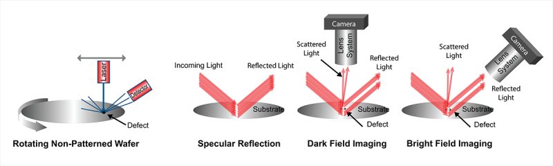
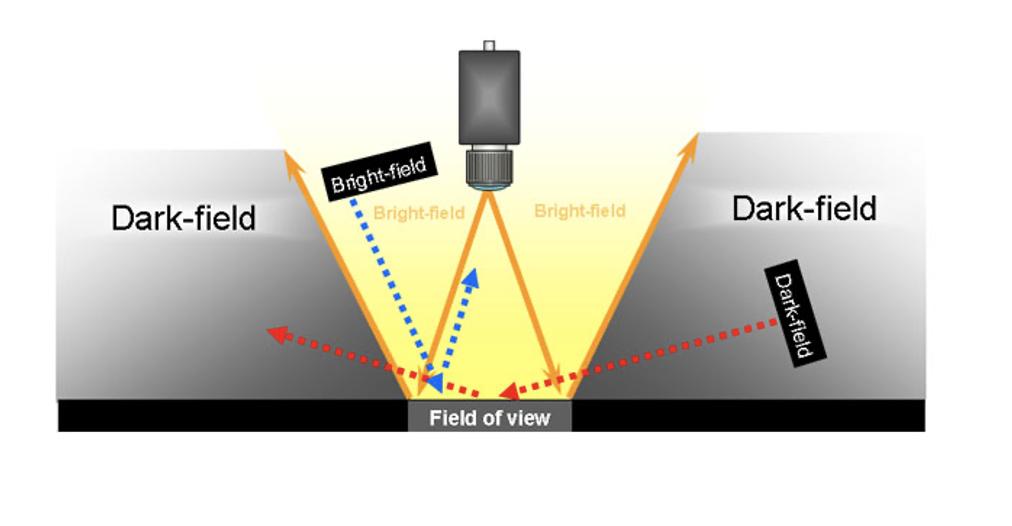
- Standard darkfield inspection with an optional brightfield channel; both modes can run concurrently for capturing and classifying a wide range of yield-critical and latent defect types in a single pass
- Optional brightfield channel specifically for detecting large substrate defects such as epi stacking faults and air pockets
- Automated defect signature detection and classification to speed identification and root-cause sourcing
- Integrated SURFmonitor capability for process optimization, surface roughness measurement, and capture of ultra-fine slip lines and scratches
- Optional backside inspection module for detecting defects that could deform wafer shape during photolithography
- Cross-model matching and correlation across the Surfscan SP1, SP2, SP3, SP A2, and SP A3 family
- Platform architecture designed with extensibility toward larger substrate formats (a dedicated Surfscan SP3 450 configuration was developed for 450mm wafers)
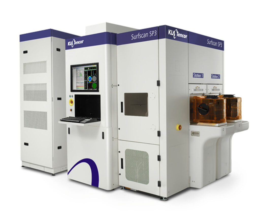
Inspection Capabilities
- Modes: Darkfield (standard) and brightfield (optional), operating concurrently
- Resolution: High-resolution (~100 megapixel) full-wafer SURFmonitor haze maps for automated capture of ultrafine slip lines, scratches, surface roughness, and grain size data Surface characterization: Surface quality characterization and surface roughness measurement integrated into the inspection workflow
- Process monitoring: Supports mapping of film thickness and roughness uniformity, and identification of annealing issues

Detectable Defect Types
- Sub-40nm particle and pattern defects
- Epi stacking faults and air pockets (large substrate defects)
- Ultra-fine slip lines and scratches
- Surface roughness and haze anomalies
- Grain size variation
- Latent reliability-impacting defects
- Backside wafer defects affecting lithographic flatness
Supported Wafer Sizes
150mm, 200mm, and 300mm, with a dedicated Surfscan SP3 450 configuration developed to support 450mm wafers for polished silicon and epitaxial silicon substrates.
Technical Specifications (summary)
Parameter | Detail |
Illumination source | Deep-ultraviolet (DUV) laser |
Defect sensitivity | Sub-40nm |
Inspection modes | Darkfield (standard), Brightfield (optional), concurrent operation |
Target process node | |
Wafer sizes | 150mm / 200mm / 300mm (450mm variant available) |
Backside inspection | Optional module |
Haze mapping resolution | ~100 megapixel full-wafer maps |
Automation | Fully automated wafer handling |
Predecessor | Surfscan SP2XP |
Successor family | Surfscan SPx/Ax series |
Applications
- Process qualification and tool qualification
- Tool monitoring
- Outgoing and incoming wafer quality control
- Process debug
- Research & development — supporting characterization and qualification of new processes during IC, substrate, and equipment development
- Incoming/outgoing wafer qualification for wafer manufacturers
- Integration with KLA’s eDR7xxx e-beam review system for defect sourcing workflows
Key Benefits
- Higher sensitivity and throughput compared to the prior-generation SP2XP platform
- Single-pass capture and classification across a wide range of defect types (darkfield + brightfield concurrently)
- Faster root-cause identification via automated defect signature detection
- Cross-generation data matching for consistent fab-wide defect metrics
- Scalable platform architecture (150mm through 450mm)
- Reduces yield loss risk by catching latent, reliability-impacting defects early
Typical Industries Served
Semiconductor, data storage, LED, photovoltaic, and other related nanoelectronics industries, plus downstream markets relying on chip reliability: automotive, IoT, 5G, consumer electronics, and industrial sectors including military, aerospace, and medical. Substrate types served span silicon, prime silicon, SOI, sapphire, glass, GaAs, SiC, GaN, InP, GaSb, Ge, LiTaO3, LiNBO3, and epitaxial wafers.