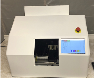
XY Scan, Bare Silicon Surface Inspection, manual load/unload system
Wafer Size: 100mm, 125mm, 150mm and 200mm
Sensitivity: 0.22um (PSL equivalent)
Size Channels: 0.22um, 0.3um, 0.5um, 1.0um, 3.0um and 5.0um+
Repeatability: < 5% variability of mean (see report)
Utilities: 115VAC @ 3amp, house vacuum and temperature-controlled cleanroom environment
Size/Weight: 30” X 30” X 30” @ 250lbs
In line configuration for Stockers; handlers
Vision
The affordable metrology solution for measuring bare silicon wafer surface defects to reliably monitor processes for contamination
Mission
Silver Sage Idaho will deliver:
A system that produces reliable, accurate and repeatable measurement data for process monitoring and troubleshooting
A system that is simple to operate, dependable, easy to maintain and has a very low cost of ownership
A system that even the smallest semiconductor industry businesses can afford to buy, use and maintain
SDM-100 System
Concept of Use
Single wafer measurements
Manual load/un-load
Table-top workspace with basic utilities (power, vacuum)
Concept of Target Users
Tool manufacture to validate tool cleanliness
R&D Lab engineers to monitor process development cleanliness
Process equipment engineers to validate tool cleanliness
Process production engineers for inline SPC sampling of monitor wafers
Concept of Target Providers
Independent semiconductor equipment sale and service companies
Equipment manufacture that would like to license SDM-100 production
SDM-100
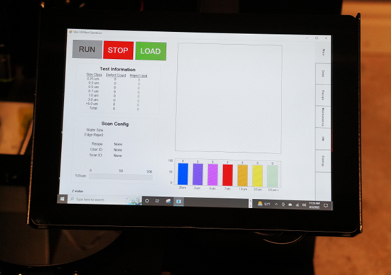
User Interface
SDM-100 User Interface Display
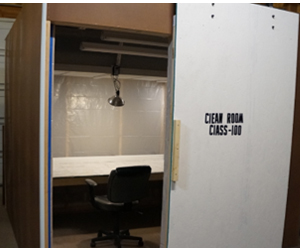
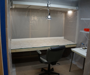
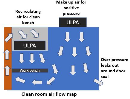
Class-100 Clean Room for calibration/testing
Clean room is air-tight to ensure positive pressure and outflow
Clean room is 100% lined with 8mil plastic for easy cleaning and air isolation
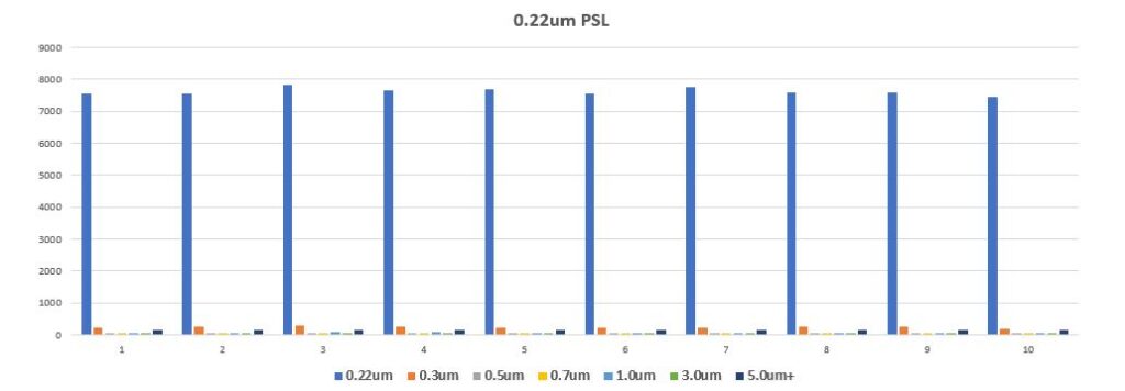
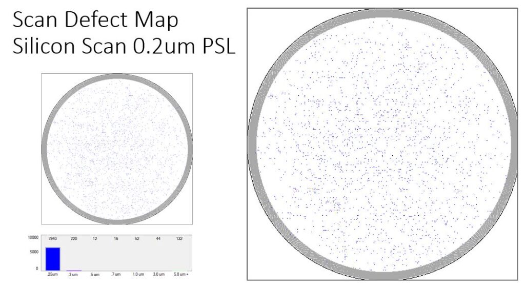
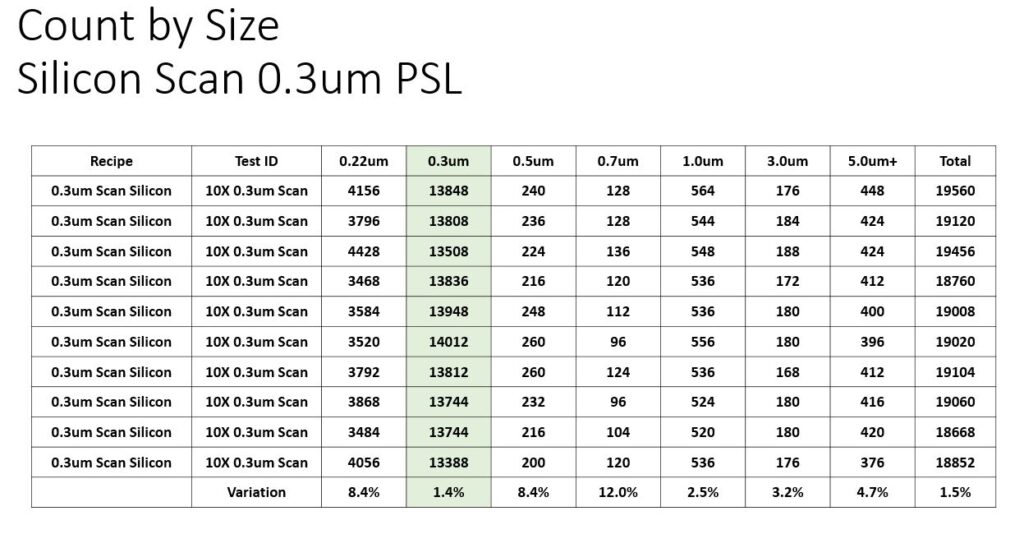
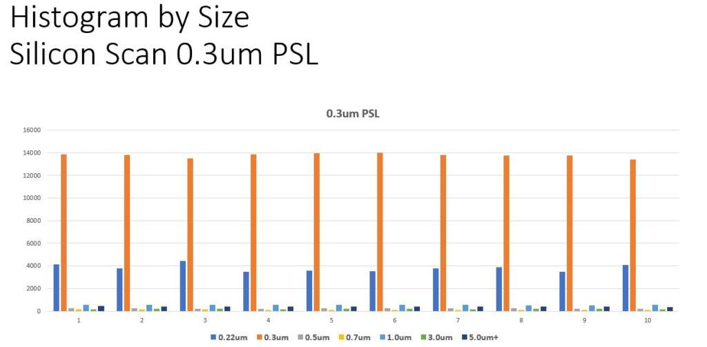
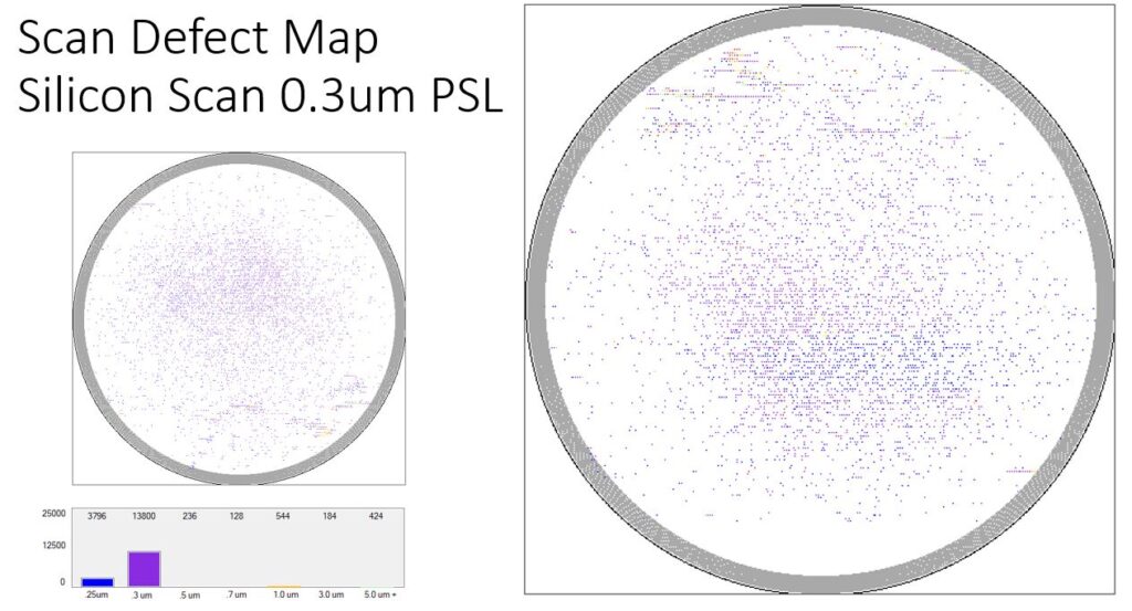
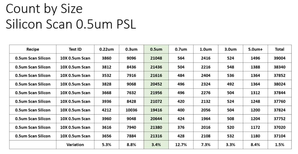
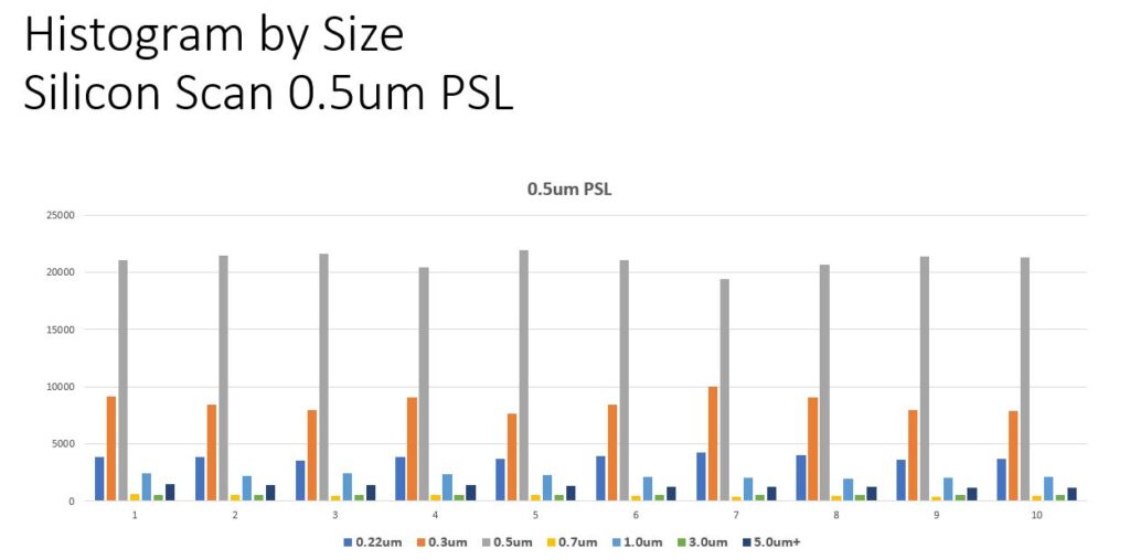
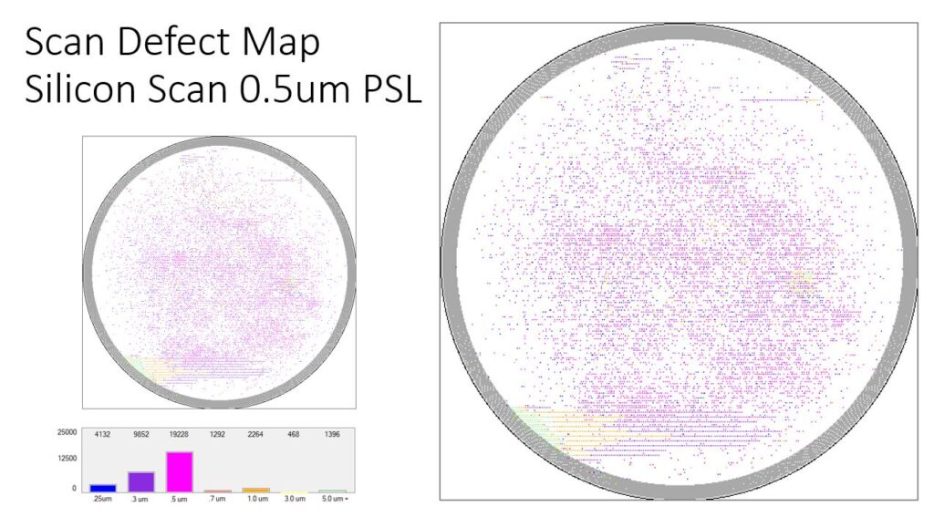
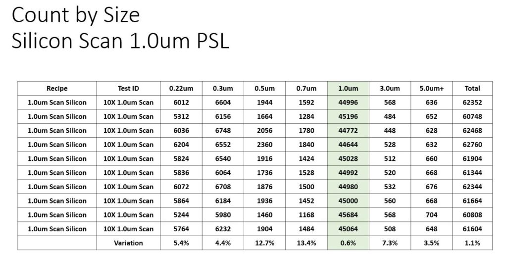
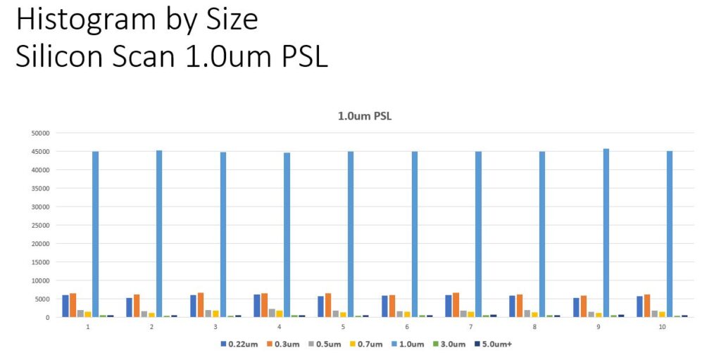
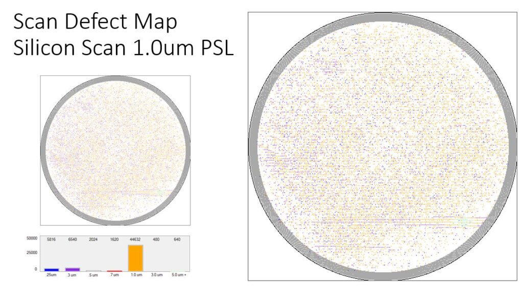
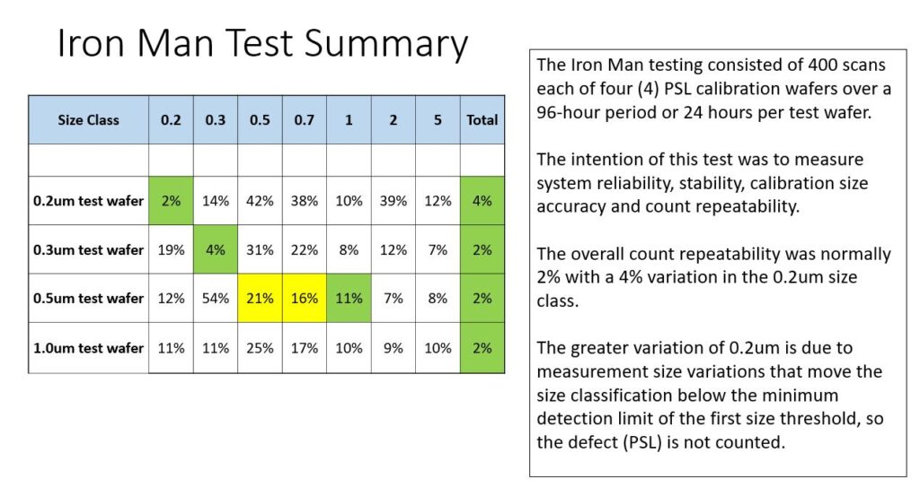
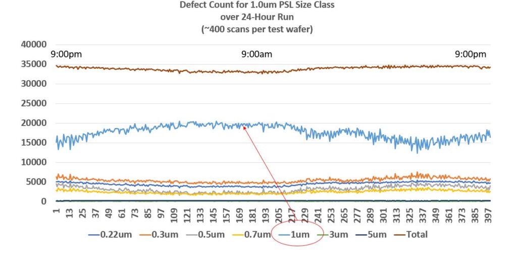
Surface Defect Monitor SDM-100 Repeatability Study (10X scans per PSL calibration wafer) August 2022
SDM-100 Repeatability Scan Summary
Repeatability of 10 scans for measured PSL size class is better than 5%
Repeatability of 10 scans for total measured wafer particles is better than 3%
PSL sizing is consistent across the full wafer (top-bottom-left-right)
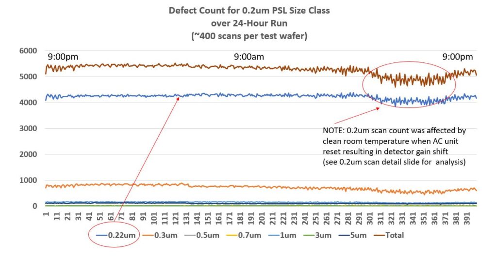
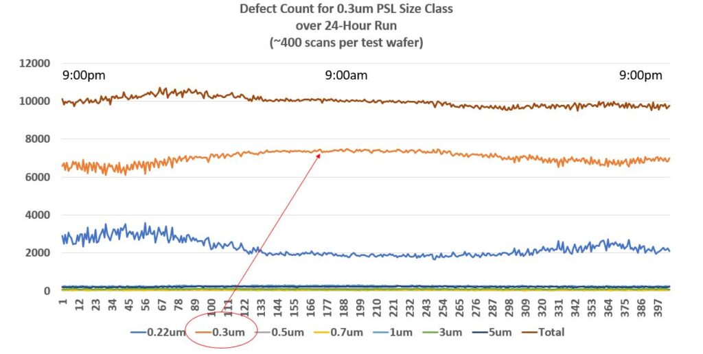
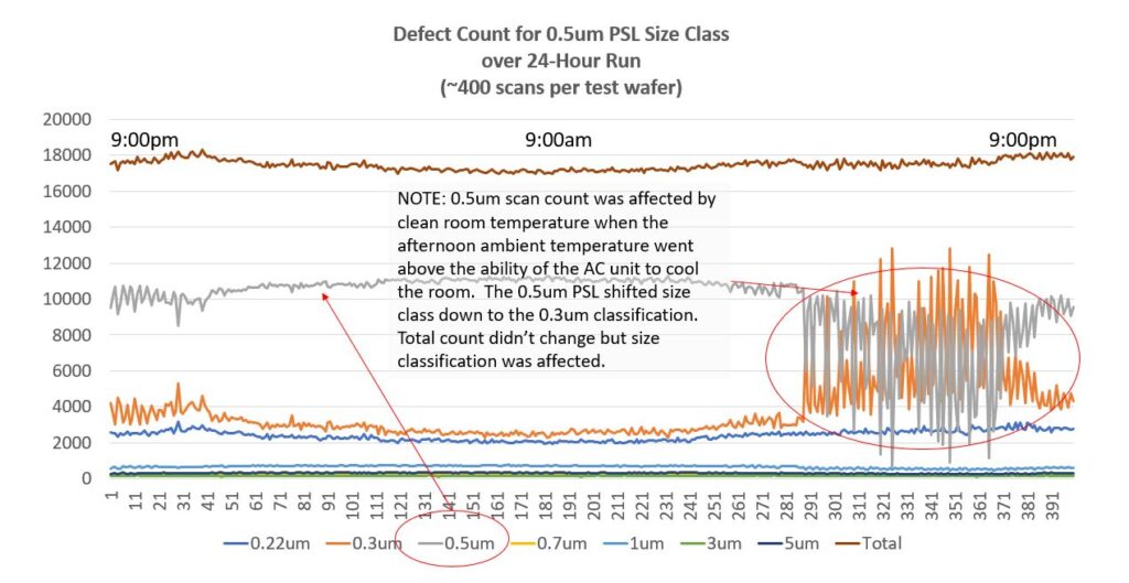
The 0.5um size repeatability was 3.4% due to some count shifting down from 0.5um to 0.3um channels caused by temperature related detector gain drift as the cleanroom AC unit cycles on/off (75F to 80F). In a better controlled cleanroom, this will not happen.