Diamond H3 Wafer Handling Robot’s
The Diamond H3 series atmospheric robots represent a significant engineering advancement in the design and reliability of wafer handling equipment. Benefiting from technologically superior components, the robots utilize ultra low inertia, high-response brushless servomotors coupled with zero-backlash Harmonic Drive® gears to achieve greatly enhanced dexterity and precision. The innovative, all-in-one, class 1 clean room compatible design incorporates the motion controller, servo amplifiers, and power supply within the robot’s industry standard footprint. High-strength structural members enable top, bottom or side mount configurations without compromising the system rigidity. A 32-bit, real-time kernel delivers accurate motion profiling along smooth continuous trajectories, while the distributed control architecture allows a seamless integration with linear tracks, prealigners, and other sub-components. Networkable RS-485 and Ethernet interfaces complement the standard RS-232 and teach pendant connections. Powerful native wafer handling and scripting languages facilitate rapid software development for embedding the robots into an OEM application environment. Comprehensive emulation of legacy robot “macro” commands offers a drop-in compatibility with a wide variety of existing semiconductor tools.
General Specification
- Wafer Size:150, 200, 300mm, or bridge Notched or flatted.
- Material: Opaque Translucent Transparent
- Thickness: 50μm~1800μm
- Warpage: less than 8mm
- Wafer Id:Top, bottom or random
- Contact: Back side or edge contact
- Carrier: FOUP, SMIF or Cassette
- Robot:JEL or compatible
- End Effector: Quartet Mechanics
- Aligner: Quartet Mechanics
- Wafer Id Reader: IOSS WID120
- LoadPort: Hirata or compatible
- Tool or Fab host communication: via SECS/GEM or TCP/IP
- Software: Standard operation software with GUI
- Function: Align and capture wafer ID, transfer wafer between carriers or to/from process module, optional flipping
Features
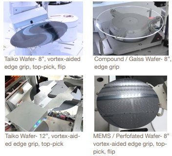
- Specializes in fragile wafer transfer: ultra-thin, Taiko, ultra-thick, warped, perforated and compound wafers (e.g. SiC)
- One machine can transfer 6”~12” multi-size and multi-type wafers
- Options: top-pick, flip, high precision, non-con- tact, Bernoulli thin wafer transfer
- Can mix and match FOUP, SMIF and Cassette
- Proprietary intelligent grippers and wafer align- ers for easy customization
Sankyo 3
-Atmospheric Wafer Handler robot
Features
- Improved Version 4th generation
- Up to 25% speed increase.
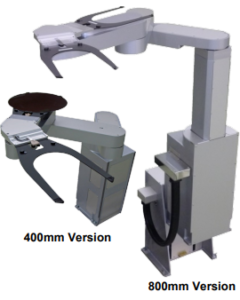
- 400mm Z-Stoke(opt. 470mm and 900mm)
- Universal Hand interface- wide variety of end effectors(with and w/o integrated mapping): Vacuum, edge-grip and passive.
- Supinator version(add. Flip-Axis).
- Small installation space-wide working area: ability to serve uop to five 300mm FOUPs without linear track axis.
- Optional vacuum and passive pre-aligner.
Specification
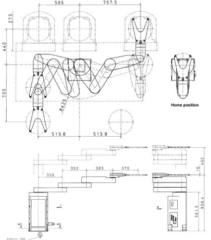
- Deg. of Freedom:5-Axis All AC Servo Controlled
- Working Range:X-axis:685 mm-685 mm,Arm Length: 350 mm; Z-Axis:400 mm (470 & 800mm );Theta-Axis:±170 deg;
- Rel. Angle:Roll1 / Roll2: ±165 deg; Rel. Angle 3rd Arm / Roll: ±275 deg
- Maximum Speed: X-Axis: 1709mm/s,Z-Axis: 700 mm/s, Theta-Axis: 6.54 rad/s,Roll-Axis: (1/2) 9.42 rad/s
- Repeatability: ± 0.05mm (ISO 9283)
- Payload 2 kg (each EE)
- Cleanliness: ISO Class1
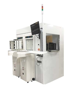
WA-E, Wafer Handler EFEM
Metrosemi provides wafer sorters/EFEMs built with in-house components, facilitating effort- less customization. Our equipment can be readily adapted to your specific needs and is ideally suited for various types of delicate wafers, including com- pound wafers (such as silicon carbide and gallium arsenide), IGBT and MEMS.Our transfer system offers high-precision place- ment, making it an excellent choice for inspection, metrology, or laser marking purposes. It is designed to be non-contact (except in exclusion zone) for contamination prevention, ensuring the mainte- nance of the highest standards of cleanliness.Our software-driven operating system, compatible with multi-wafer sizes and diverse carrier types, is built upon a modular software platform that guarantees both flexibility and scalability. To ensure an intuitive user experience, we’ve incor- porated a visual animation interface. Compliance with SEMI SECS/GEM standards is a key feature, facilitating optional.
General Specification
- Wafer Size:150, 200, 300mm, or bridge Notched or flatted.
- Material: Opaque Translucent Transparent
- Thickness: 50μm~1800μm
- Warpage: less than 8mm
- Wafer Id:Top, bottom or random
- Contact: Back side or edge contact
- Carrier: FOUP, SMIF or Cassette
- Robot:JEL or compatible
- End Effector: Quartet Mechanics
- Aligner: Quartet Mechanics
- Wafer Id Reader: IOSS WID120
- LoadPort: Hirata or compatible
- Tool or Fab host communication: via SECS/GEM or TCP/IP
- Software: Standard operation software with GUI
- Function: Align and capture wafer ID, transfer wafer between carriers or to/from process module, optional flipping
Features
- Specializes in fragile wafer transfer: ultra-thin, Taiko, ultra-thick, warped, perforated and compound wafers (e.g. SiC)
- One machine can transfer 6”~12” multi-size and multi-type wafers
- Options: top-pick, flip, high precision, non-con- tact, Bernoulli thin wafer transfer
- Can mix and match FOUP, SMIF and Cassette
- Proprietary intelligent grippers and wafer align- ers for easy customization