PMM Data Analysis Tool
MetroSemi has developed a novel method known as the PMM method for estimating the mean and bounds of functional data analysis. The newly developed method has been demonstrated to be highly accurate and significantly faster than previous state-of-the-art methods. Utilizing this method, precise mean and bound characteristics curves can be generated for a variety of active and passive electronic devices, including diodes, transistors, resistors, inductors, and capacitors. Device characteristic curves can originate from SPICE simulations or laboratory-measured I-V sweeps collected across various processes and temperatures. This tool can assist semiconductor designers in fine-tuning their designs or in generating fabrication recipes to achieve higher device yield and reliability. This research work was published and presented at the 7th IEEE Electron Devices Technology and Manufacturing (EDTM) Conference in 2023, held in Seoul, South Korea.
Applications
Characteristic Mean and Bound of Wafer bow profiles:
The figure below illustrates the mean estimation of 116 Zener diodes. In this context, the 116 blue curves represent the characteristics of Zener diodes under varying Process, Voltage, and Temperature (PVT) conditions, which are used as inputs for the PMM tool. A single red curve represents the mean curve generated by the PMM method, and the two outermost curves represent the bounds produced by the PMM tool, which serve as its outputs. The PMM output characteristic curves encompass all the input characteristic curves. Designers can now fine-tune their design recipes based on the PMM outputs.
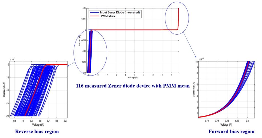
Characteristic Mean and Bound of Zener Diodes:
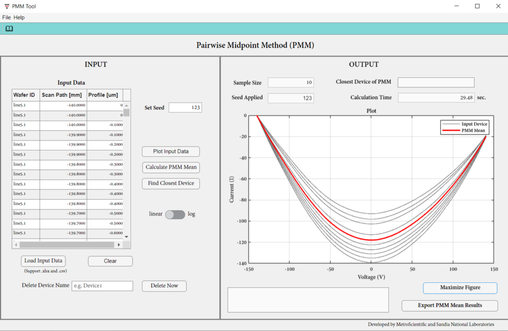
The figure below illustrates the mean and bound estimations of wafer bow profiles. In this scenario, the 10 gray curves represent the bow characteristics of semiconductor wafers at different temperatures, ranging from room temperature to 500°C. A single red curve represents the mean curve generated by the PMM method, while the two outermost curves represent the bounds produced by the PMM tool, serving as its outputs. These PMM output characteristic curves encompass all the input characteristic curves. Now, semiconductor material scientists can fine-tune and optimize the physical properties of the wafer based on the PMM outputs.
Computational Storage Architecture and Programming Model
We develop embedded systems (both software and hardware), FPGA (Xilinx, Intel, etc.)/ASIC design and verification, RTL reusable design, storage accelerators, and many other cutting-edge technologies. Recently we completed our projects on complex technologies which include near memory computation, Smart SSD, Computational Storage Drive, Embedded Ethernet Subsystem, etc.