FSM 128 Film Stress & Wafer Bow Measurement System
Introduction
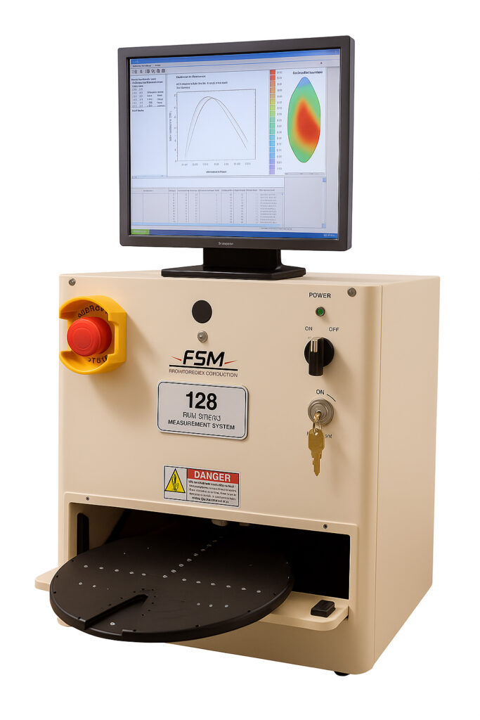
The FSM 128 is an advanced system for precise wafer stress, curvature, and bow measurement. Utilizing a non-contact technique, it ensures accuracy and reliability. Available in Film Stress & Wafer Bow Measurement System, it supports wafers up to 300mm, providing 2D/3D stress mapping with intuitive operation.
Specifications
Film Stress Range: 1 MPa to 1.4 GPa (for Si wafers with ≥1µm bow/curvature change)
Mapping: 32 scan lines (6 recommended) with 40 data points/mm
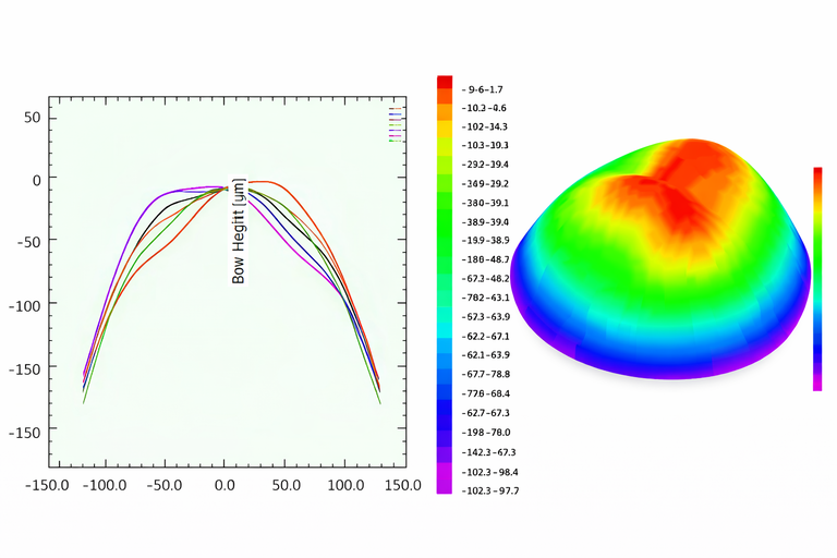
Bow Measurement: Measures bow heights up to 2000µm
Advanced Optics: Patented dual laser switching for accuracy
Software: Windows 7–11 compatibility, data export to Excel™, JPEG maps
Operating Conditions: Ambient temperature
Measurement Method: Non-contact laser scanning
Wafer Compatibility:
FSM 128NT: 50mm to 200mm
FSM 128L: 50mm to 300mm
Wafer thickness: <5mm
Scanning: High-precision single scan and programmable multiple diametric scans for 2D/3D mapping
Repeatability: 1% (1 sigma) on a 20m curvature mirror standard
Accuracy: <2.5% on a 20m radius curvature mirror
Laser Class: Class 1
FSM 128
Data and Connectivity
Export results to Excel™ or JPEG.
System Requirements
Computer: Intel Core i5 or later, 2GB RAM, 1TB hard drive, 4 USB ports, 2 Ethernet ports.
Dimensions & Weight
FSM 128NT: 14″ (W) x 20″ (D) x 16″ (H), 55 lbs
FSM 128L: 14″ (W) x 28″ (D) x 16″ (H), 60 lbs
Power Requirements
110V/220V; 20A
Notes
Wafer bow is the deviation of the center point of the wafer’s front surface when supported on a 3-point system.
Repeatability and accuracy depend on film type, thickness, and substrate.
Semiconductor, Optoelectronics & FPD Application
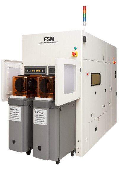
FSM 128C2C Automated Film Stress & Wafer Bow Measurement System
Introduction
The FSM 128C2C series is a fully automated system designed for stringent production environments, including next-generation devices in 300mm fabs, III-V, and MEMS industries. It offers robotic cassette handling and supports wafers ranging from 150mm to 300mm. Configurations include open cassette, SMIF, and mini-environment modules.
Specifications
Film Stress Range: 1 MPa to 1.4 GPa (Si wafers with ≥1µm bow/curvature change)