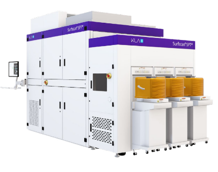
Surfscan® SP7XP
Unpatented Wafer Inspection Solution for Power Device Applications
The Surfscan® SP7XP unpatented wafer inspection system facilitates qualification and monitoring of processes and tools for IC, wafer, equipment and materials manufacturers for ≤5nm logic and advanced memory design nodes. With industry-best 12.5nm sensitivity and high throughput, the Surfscan SP7XP provides a single tool solution for both R&D pathfinding applications and process monitoring during high volume manufacturing. Built on the industry-standard Surfscan® platform, the Surfscan SP7XP delivers ultimate sensitivity to critical defects and enhanced defect classification for bare wafers, smooth and rough films, and fragile resists and litho stacks, including those used for EUV lithography. By discovering and identifying critical defects and surface quality issues, the Surfscan SP7XP enables faster identification of process and tool issues, driving faster ramp, higher yield and improved fab profitability. As an extension of the Surfscan SP7, the Surfscan SP7XP incorporates new hardware technologies and innovative algorithms that enable enhanced capability, including:
▪ Ultimate sensitivity for advanced design node R&D pathfinding by IC fabs, wafer houses and equipment manufacturers
▪ High throughput for cost-effective monitoring during high volume manufacturing of advanced design node devices
▪ Capture of unique defects types using new inspection modes for support of a broad range of process monitoring applications
▪ Image based defect classification using revolutionary machine learning algorithms for faster time to root cause
Surfscan SP7XP Advanced Features
Defect Sensitivity
- New 12.5nm inspection mode and low noise sensors provide the inspection sensitivity required for R&D pathfinding at leading-edge design nodes, including development of logic devices using gate all around transistors.
- The new Phase Contrast Channel (PCC) provides enhanced signal for improved capture of defect types with weak scattering in the normal or oblique channel, such as shallow bumps or residue.
- The Normal Illumination (NI) inspection channel utilizes an independent objective to optimize capture of defects of interest not found in the oblique channel. NI finds unique non-cleanable defects, like embedded deformities and scratches, and provides higher capture of sliplines, residue and optical microscope visible (OMV) defects at higher productivity compared to the normal channel on Surfscan SP5XP.
Defect Classification

- Image Based Classification (IBC) leverages an advanced TDI camera and revolutionary machine learning algorithms to accurately classify detected defects, reducing the time to root cause. IBC greatly reduces the time required for classification recipe setup compared to previous- generation classification engines, with >60% time savings demonstrated for some layers. Enhanced Signal Detection (ESD), a key feature of IBC, leverages information from all inspection channels to improve classification of defects such as scratches and epi stacking faults (ESF), helping engineers better understand and improve processes.
- The Z7TM multi-channel defect classification engine provides a unique classification solution for embedded defects in 3D NAND and other thick film applications. The Z7 classification data facilitates troubleshooting of excursion root causes and correlates defect characteristics to inline yield impact. In addition to reducing time to root cause, Z7 reduces the need for SEM/FIB and additional test wafers when troubleshooting process issues.
Defect Sensitivity
- New 12.5nm inspection mode and low noise sensors provide the inspection sensitivity required for R&D pathfinding at leading-edge design nodes, including development of logic devices using gate all around transistors.
- The new Phase Contrast Channel (PCC) provides enhanced signal for improved capture of defect types with weak scattering in the normal or oblique channel, such as shallow bumps or residue.
- The Normal Illumination (NI) inspection channel utilizes an independent objective to optimize capture of defects of interest not found in the oblique channel. NI finds unique non-cleanable defects, like embedded deformities and scratches, and provides higher capture of sliplines, residue and optical microscope visible (OMV) defects at higher productivity compared to the normal channel on Surfscan SP5XP.