Thickness Measurement of Two Bonded Wafers and TSV Depth Measurement using FSM 413 SA (DP)
I. Objective
The objective of these measurements is to demonstrate FSM 413’s capability to measure total thickness, individual layer’s thickness of two bonded wafer and TSV depth .
II. Sample description:
6 4 inch wafers were was received. Detail of sample description is on the table below.
Table 1. Sample Description
No. | Wafer | Wafer ID | Wafer Type | Wafer Size/ used area(%) | Sample Description |
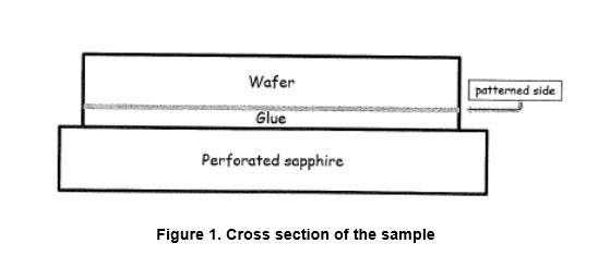
1 | Efraim 447 | PM022415 | GaN on SiC | 100mm/90% | GaN on SiC wafer (90mm) bonded to perforated sapphire (100mm) |
2 | Efraim 447 | PV023137 | GaN on SiC | 100mm/90% | GaN on SiC wafer (90mm) with via and Ni bonded to perforated sapphire (100mm) |
3 | Efraim 447 | QH020311 | GaN on SiC | 100mm/90% | GaN on SiC wafer (90mm) after backgrind ( Ra<0.1 um) bonded to perforated sapphire (100mm) |
4 | Hellus418 | AY195037 | GaAs | 100mm/95% | GaAs patterned wafer (100 mm) bonded to perforated sapphire (150mm) |
5 | Hellus418 | AY218045 | GaAs | 100mm/95% | GaAs patterned wafer (100 mm) after chem etch bonded to perforated sapphire (150mm) |
6 | NoMask455 | CA848020 | GaAs | 100mm/95% | GaAs patterned wafer (100 mm) after backgrind (Ra< 0.1 um) bonded to perforated sapphire (150mm) |
III. Demo System Setup:
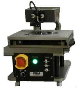
Metrology tool: FSM 413SA (DP) 300MM SEMI-AUTOMATED HIGH RESOLUTION SUBSTRATE THICKNESS MAPPER (For 100mm, 150mm, 200mm and 300mm Wafers)- DUAL PROBE SYSTEM. Microscope (10X) and Camera option is chosen to see the image of via for measurement.
IV. Summary
The average thicknesses of individual layers and total layer at 29 points for GaN on SiC wafer are in table 2 and table3. The thickness of individual layers is measured by single probe except glue layer and the total thickness is measured by dual probe. The glue thickness is measured by subtracting individual thicknesses from total thickness. If the bottom probe hits the hole of the perforated sapphire layer accidently, it can not measure the thickness of sapphire layer due to no interference signal. The two signal at the interface between SiC and glue and at the interface between glue and sapphire is too close to be separated in some positions. This caused unstable reading and a large standard deviation for the thickness of sapphire layer and wafer.
TSV depth of wafer 2 is measured by taking the difference between the maximum and the minimum distances of echo signal from reference signal as the probe is moved over TSV by a step of 25 μm.
The average thicknesses of individual layers and total layer at 16 points for GaAs wafer are in table 4. The thickness of individual layers is measured by single probe except glue layer and the total thickness is measured by dual probe. The glue thickness is measured by subtracting individual thicknesses from total thickness.
Table 2. Average thickness of individual layers and total layer for wafer 1 and wafer 3.
Wafer ID | Sapphire (μm) | GaN on SiC (μm) | Glue (μm) | Total (μm) |
PM022415 | 715.1 | 522.2 | 14.0 | 1251.3 |
QH020311 | 711.8 | 123.1 | 21.0 | 855.9 |
Table 3 Average TSV depth and total thickness of wafer 2.
Wafer ID | TSV depth (μm) | Total (μm) |
PV023127 | 84.1 | 850.9 |
Table 4 Average thickness of individual layers and total layers for wafer 4, wafer 5 and wafer 6.
Wafer ID | Sapphire (μm) | GaAs (μm) | Glue (μm) | Total (μm) |
AY195037 | 713.7 | 632.7 | 21.4 | 1367.8 |
AY278046 | 714.1 | 99.1 | 20.7 | 833.9 |
CA848020 | 712.7 | 124.6 | 23.0 | 860.2 |
- Data
Table 5. 3 trial measurements for wafer 1(PM022415)
| Position | Trial 1 | Trial 2 | St. Deviation | ||||||||||
No. | X (mm) | Y(mm) | Sapphire | GaN | Glue | Total | Sapphire | GaN | Glue | Total | Sapphire | GaN | Glue | Total |
1 | 0 | 0 | 714.4 | 522.5 | 14.4 | 1251.3 | 714.0 | 522.5 | 14.9 | 1251.4 | 0.3 | 0.2 | 0.3 | 0.0 |
2 | 0 | -12.7 | 714.7 | 522.1 | 13.4 | 1250.2 | 714.8 | 522.3 | 13.9 | 1251.0 | 0.5 | 0.3 | 0.5 | 0.4 |
3 | 0 | -25.4 | 715.1 | 522.3 | 13.5 | 1250.8 | 714.6 | 522.5 | 14.4 | 1251.4 | 0.4 | 0.1 | 0.6 | 0.3 |
4 | 0 | -38.1 | 716.9 | 521.7 | 12.1 | 1250.6 | 715.9 | 521.7 | 13.5 | 1251.1 | 0.5 | 0.2 | 0.8 | 0.3 |
5 | 38.1 | -12.7 | 712.6 | 521.9 | 18.5 | 1252.9 | 711.6 | 521.8 | 19.5 | 1252.9 | 0.5 | 0.2 | 0.6 | 0.1 |
Min |
| 712.1 | 521.4 | 9.7 | 1248.9 | 711.6 | 521.6 | 10.1 | 1249.3 | 0.2 | 0.1 | 0.2 | 0.2 | |
Ave |
| 715.1 | 522.1 | 13.9 | 1251.1 | 715.2 | 522.2 | 14.1 | 1251.4 |
|
|
|
| |
Max |
| 717.8 | 523.0 | 18.5 | 1253.7 | 717.7 | 523.2 | 19.5 | 1253.6 |
|
|
|
| |
StDev |
| 1.4 | 0.3 | 2.0 | 1.1 | 1.6 | 0.4 | 2.1 | 1.1 |
|
|
|
| |
TTV |
| 5.8 | 1.7 | 8.7 | 4.7 | 6.2 | 1.6 | 9.5 | 4.3 |
|
|
|
| |
Table 6 TSV depth measurement for wafer 2(PV023127)
| Position | TSV Depth (μm) |
| |||
No. | X (mm) | Y (mm) | Trial 1 | Trial 2 | Tria; 3 | St. Deviation |
1 | -0.54 | 0.05 | 83.8 | 78.9 | 83.5 | 2.7 |
2 | 0.65 | -12.53 | 80.7 | 80.2 | 79.6 | 0.5 |
3 | -0.26 | -25.37 | 80.1 | 77.8 | 79.0 | 1.2 |
4 | 0.38 | -38.08 | 80.0 | 82.5 | 80.6 | 1.3 |
5 | 37.14 | -12.56 | 88.4 | 88.5 | 88.1 | 0.2 |
Min | – | – | 80.0 | 77.8 | 78.4 |
|
Ave | – | – | 84.3 | 84.0 | 84.1 |
|
Max | – | – | 90.8 | 90.6 | 91.4 |
|
StDev | – | – | 3.4 | 3.4 | 3.6 |
|
TTV | – | – | 10.8 | 12.8 | 13.0 |
|
Table 7 Total thickness measurement for wafer 2(PV022127)
| Position | Total thickness (μm) |
| |||
No. | X (mm) | Y (mm) | Trial 1 | Trial 2 | Trial 3 | St. Dev. |
1 | 0 | 0 | 849.2 | 848.7 | 848.6 | 0.3 |
2 | 0 | -12.7 | 850.8 | 850.7 | 850.8 | 0.0 |
3 | 0 | -25.4 | 852.3 | 851.7 | 850.8 | 0.7 |
4 | 0 | -38.1 | 852.6 | 852.5 | 853.0 | 0.2 |
5 | 38.1 | -12.7 | 852.9 | 852.5 | 853.0 | 0.3 |
Min | – | – | 849.2 | 848.7 | 848.6 |
|
Ave | – | – | 851.0 | 851.0 | 850.8 |
|
Max | – | – | 852.9 | 852.6 | 853.0 |
|
StDev | – | – | 1.09 | 1 | 1.16 |
|
TTV | – | – | 3.75 | 3.9 | 4.44 |
|
VI. Measurement Principle
- Thickness Measurement By Single Probe
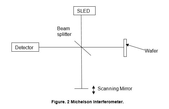
The basic principle of the tool is utilizes the low coherent SLED light source in Michelson interferometer as shown in Figure 2. One branch of the splitted beam goes to the measurement stage and another branch of the splitted beam goes to scanning mirror which moves at the frequency of 10Hz with stroke 5mm. The schematic of dual probes of FSM 413-SA-DP is shown in Figure 3. Each probe has a reference mirror, which sends the light back to detector to make a reference signal. These reference signals are useful for warp, TSV depth, trench depth, bump height, and total thickness measurement. Light reflected from reference mirror, and the interface of each layers of wafer produces interference signals in the each probe as it passes through. The typical interference signal of the single probe is in Figure. 4. The distance between the second and the third peak in single probe is used to calculate the thickness of the sapphire in bottom probe or the thickness of wafer in top probe. The measurement with single probe necessitates knowledge of the refractive index of each layer to calculate its thickness.
2.Total Thickness Measurement By Dual Probe
Dual probe measurement uses a block gauge to determine L=A+B+BG first, where A is the distance between reference mirror signal and top surface signal in top probe, B is the distance between reference mirror signal and bottom surface signal in bottom probe at the block gauge, and BG is the known thickness of metal block gauge. The typical signal at block gauge is in Figure 5. Then, the thickness of sample can be calculated from t=L-a-b, where a is the distance between reference mirror signal and top surface signal in top probe and b is the distance between reference mirror signal and bottom surface signal in bottom probe at the sample. Refer to Figure. 6. For dual probe measurement, one doesn’t need to know the refractive index beforehand.
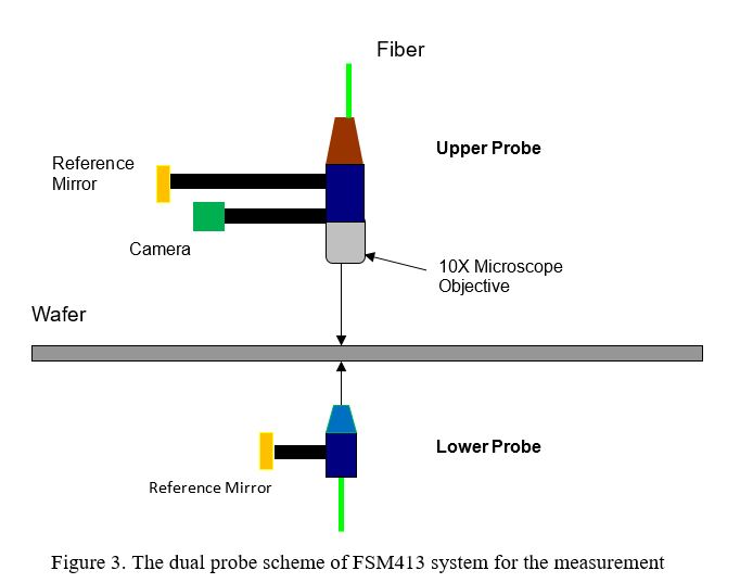

Figure 4. A typical interference signal of the wafer for the top (a) and bottom (b) probe. a is a distance between the reference mirror signal and the top surface signal of the wafer. b is a distance between the reference mirror signal and the bottom surface signal of the sample.

Figure 5. A typical interference signal at block gauge for the top (A) and bottom (B) probe. A is a distance between the reference mirror signal and the top surface signal of the block gauge. B is a distance between the reference mirror signal and the bottom surface signal of the block gauge.
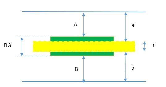
Figure 6.The procedure of the thickness measurement with dual probe is the following: first, it determines L=A+B+BG at the position of block gauge. Then, it measures sample thickness( t=L-a-b) at the sample position. The line square in the picture is block gauge of known thickness (500μm) and the dotted square is sample thickness.
