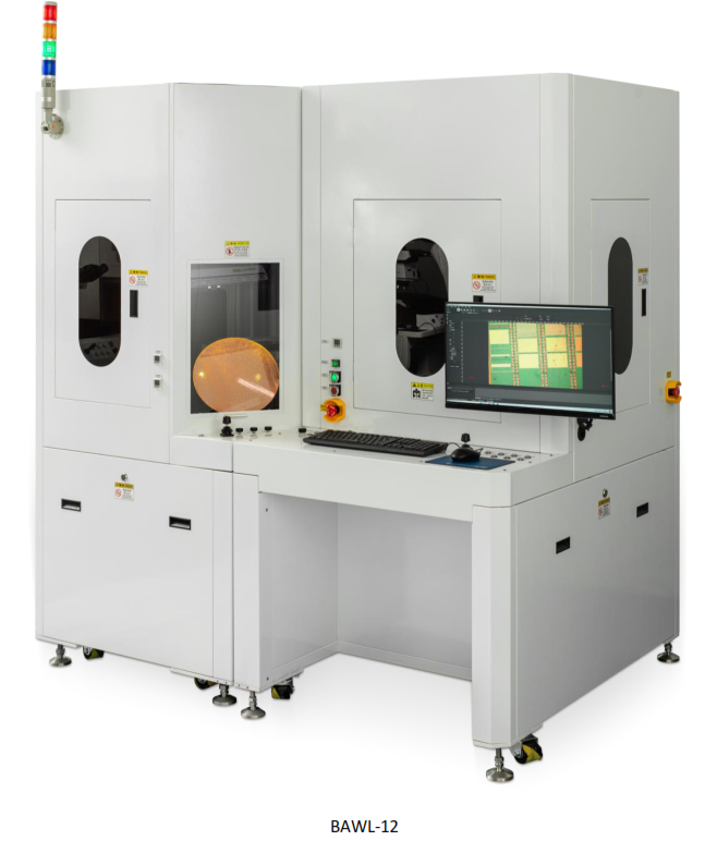
The BAWL-12 Wafer Inspection System is your ultimate solution for advanced semiconductor wafer inspection. With fully automated wafer handling, high-definition optical imaging, and cutting-edge analysis capabilities, the BAWL-12 series sets a new benchmark in wafer defect detection and process optimization.
Key Features
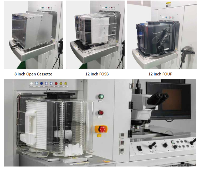
EFEM System: Smart Wafer Handling
Automated loading and unloading with precision mechanical arms.
Compatible with FOUP, FOSB, Smif Pod, and Open Cassettes.
Advanced barcode scanning and RFID for seamless wafer identification.
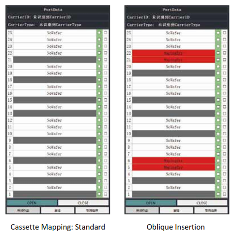
High-Precision Mapping
Layer-by-layer scanning for accurate wafer position tracking.
Detects tilted or misaligned wafers with 100% accuracy.
Instant alarms for abnormal conditions.
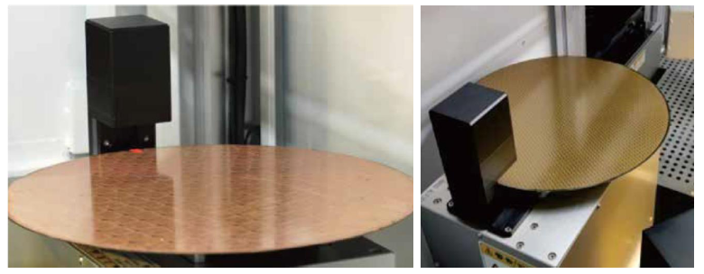
Non-Contact Wafer Pre-Alignment
Optical system for precise center and notch/flat location.
Efficient, automated mechanism for fast, accurate positioning.
Supports various materials: Si, SiC, EMC, Glass, and more.
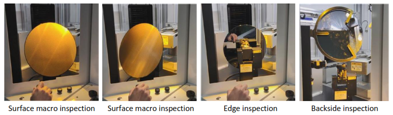
360° Macro Inspection
Full-surface inspection including front, back, and edges.
Multi-angle viewing via a responsive control lever.
Customizable LED lighting options: white, yellow, and green.
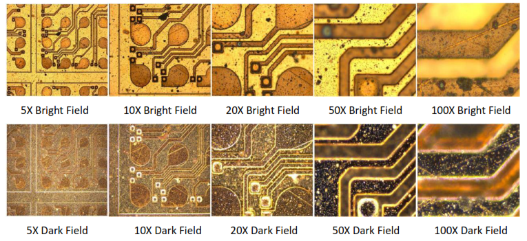
Ultra-Wide Micro Inspection
25mm ultra-wide field of view for detailed imaging.
High-resolution imaging with polarization and DIC contrast.
Electric Precision Control
Electrically controlled objective and diaphragm for optimal accuracy.
Front-panel controls for ergonomic operation.
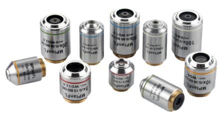
APO Objectives with Long Working Distance
High-transmittance lenses with superior color correction.
Non-destructive testing for multiple observation modes (bright field, dark field, polarization, DIC).
Advanced Image Analysis Software
Automatic image stitching, depth fusion, and 3D measurement.
Features auto-focus, particle counting, and real-time visualization.
Compatible with 64-bit Windows systems.
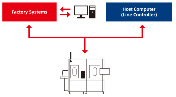
SECS/GEM Data Communication
Seamless integration with MES systems for real-time monitoring.
Wafer OCR for process tracking with unique wafer IDs.
Power-outage protection ensures data integrity.
Reliable & Safe Design
High operational stability and transmission rates.
Built-in UPS, vacuum holding system, and safety interlocks.
Complies with SEMI industry standards.
Technical Performance
Parameter
Specification
Operating Time
>95%
Chip Rate
1/100000
Maintenance Time
≤4 hours
Mean Time Between Errors
≥240 hours
System Specifications
Feature
BAWL-12 MS
BAWL-12 AS
BAWL-12 RAS
Wafer Size
200mm/300mm
200mm/300mm
200mm/300mm
Wafer Thickness
250-1000um
250-1000um
300-1000um
Loadport
1
1 or 2
1 or 2
Wafer Pre-Alignment
Non-contact
Non-contact
Non-contact
Macro Inspection
✓
✓
✓
Micro Inspection
✓
✓
✓
Image Analysis Software
Optional
Optional
✓
SECS/GEM Protocol
Optional
Optional
✓
Wafer Review System
–
Optional
✓
Power Requirements:
220V, 50Hz, 16A (MS/AS) | 220V, 50Hz, 32A (RAS)
CDA: 0.4–0.6 MPa | VAC: -70 to -90 kPa
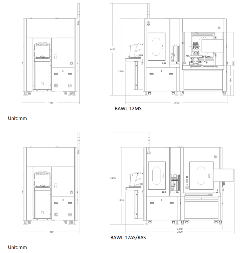
Dimensions:
1-Port: 2400mm (W) × 1400mm (D) × 2350mm (H)
2-Port: 2400mm (W) × 2050mm (D) × 2350mm (H)
Additional Features:
High-eyepoint wide-field eyepiece with micrometer.
Adjustable trinocular head (5–35°) for user comfort.
Manual or automatic focusing with real-time adjustments.
Optional accessories: filters, polarizers, DIC kits, and professional inspection software.
Dimension
Why Choose the BAWL-12 Series?
High Accuracy: Non-contact optical precision for reliable results.