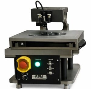
FSM 413 MOT Wafer Thickness Measurement System Desktop System with Automatic X-Y Stage Non Contact Wafer Thickness Metrology for ultra thin backgrind or chemically etched wafers, Measures patterned, bumped wafers on tapes or bonded on carriers, for stacked die and MEMS Applications
The FSM 413 Echoprobe TM sensor uses a patented infrared (IR) interferometry technique that provides a direct and accurate substrate thickness and total thick- ness variation (TTV) measurement of thick to ultra-thin wafers. Configured as a Single Probe system, several materials transparent to the IR beam, such as Si, GaAs, InP, SiC, Glass, Quartz and many polymers, are readily measured. Sub- strate thickness of conventional wafers with patterns, tapes, bumps or bonded wafers mounted on carriers can be determined with high precision and accuracy. When configured as a Dual Probe system, the FSM413 also provides measure- ments of the total thickness of the wafer, including substrate thickness and the patterned height thickness in cases the beam cannot penetrate through the materi- al. Options are available to measure trench depth and via holes, including high aspect ratio trenches and vias in MEMS type applications. Various specialized MEMS applications including membrane metrology and Bump Height metrology are also optionally available.
6Non-contact IR interferometry. Single or Dual Probes available
Wafer size:
up to 150, 200, or 300mm available, Customized wafer size also available
Substrate:
Si, GaAs, InP, Quartz, Glass, Sic, Sapphire
Thickness range:
15 to 780μm for Single Probe measurement up to 3mm for Dual Probe (Total thickness) Manual
Repeatability:
0.1 μm (Display) 0.2 μm (1 o) in Single Probe** Mode 0.7μm (1 o) in Dual Probe** Mode
Measurement Points:
Programmable
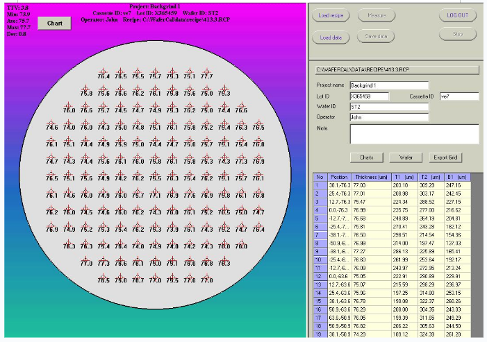
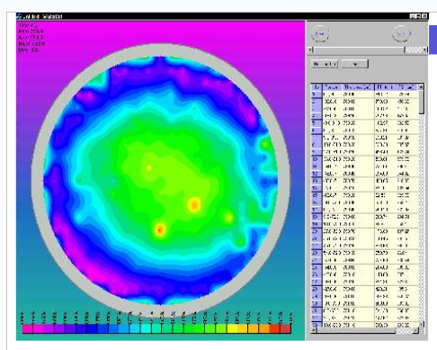
Substrate Thickness Results:
TTV, Mean, Maximum, Minimum, StDev, 2D and 3D Color Maps
Single Probe
15 ~ 780um
Dual Probe
~ 3mm
Wavelength:
1.3±0.03μ
Thin Film Option Thickness Range:
1 to 25µm
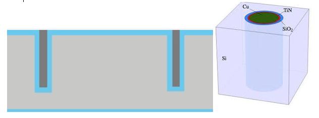
TSV
Aspect Ratio
< 10
CD diameter
> 8um
CD repeatability
0.1um
Via depth
> 50um (other configurations are available for smaller depth)
Via depth repeatability
0.2um
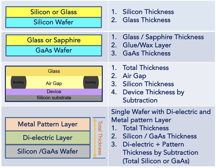
Thickness Measurement-Type of material
A. Opaque: Silicon, GaAs, InP, GaN
B. Transparent: SiC, Glass, Sapphire (boro silicate, pyrex, quartz),
C. Bonded/Sandwich: Silicon on grinding or mounting tape Silicon on silicon, glass or others
D. Bumps or Trenches (topography) Step height and above surface, Cavity, grooves and below surface
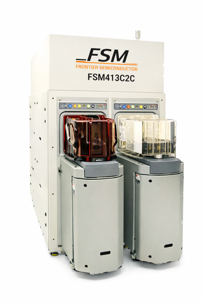
FSM 413C2C
FSM 413C2C
The FSM 413 EchoprobeTM sensor provides a direct and accu- rate map of substrate thickness and total thickness varia- tion (TTV) of thick to ultra-thin wafers. It uses a patented Infrared (IR) Interferometric Technique to measure materi- als transparent to the IR beam, such as Si, GaAs, InP, SiC, Glass, Quartz, Sapphire and many polymers. Substrate thickness of conventional wafers with patterns, tapes, bumps or bonded wafers mounted on carriers can be deter- mined with high precision and accuracy. When equipped with as Dual Probe system, the FSM413 also provides meas- urements of the total thickness of the wafer stack including non-transparent materials such as metals. Options are available to measure the wafer warp, trench depth, trim height and depth, and via hole depth.
Measures Substrate Thickness in Multiple Layers using Non-contact Optical System
High Precision XY Stage (0.5m) (optional)
Pattern Recognition (optional)
Robotic Handling System
Programmable Data Points
Measures Silicon Via Depth with Microscope Option
Excellent Repeatability & Reproducibility
Specifications
Spot size:
6μ ~40μ
Working distance:
~ 20mm
Si Thickness range :
Single Probe
15 ~ 780um
Dual Probe
~ 3mm
Wavelength:
1.3±0.03μ
FSM 413 Thickness Measurement System Working Principle
Measurement Principle
Thickness Measurement By Single Probe
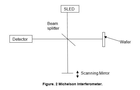
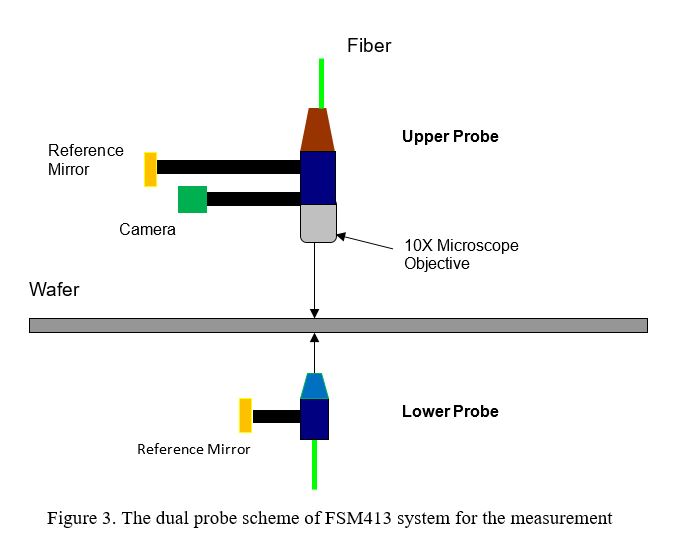
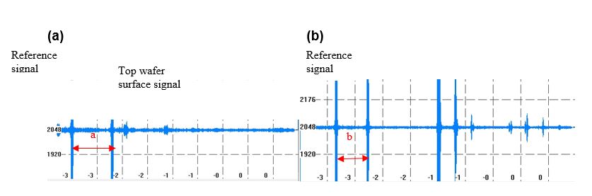
The basic principle of the tool is utilizes the low coherent SLED light source in Michelson interferometer as shown in Figure 2. One branch of the splitted beam goes to the measurement stage and another branch of the splitted beam goes to scanning mirror which moves at the frequency of 10Hz with stroke 5mm. The schematic of dual probes of FSM 413-SA-DP is shown in Figure 3. Each probe has a reference mirror, which sends the light back to detector to make a reference signal. These reference signals are useful for warp, TSV depth, trench depth, bump height, and total thickness measurement. Light reflected from reference mirror, and the interface of each layers of wafer produces interference signals in the each probe as it passes through. The typical interference signal of the single probe is in Figure. 4. The distance between the second and the third peak in single probe is used to calculate the thickness of the sapphire in bottom probe or the thickness of wafer in top probe. The measurement with single probe necessitates knowledge of the refractive index of each layer to calculate its thickness.
2.Total Thickness Measurement By Dual Probe
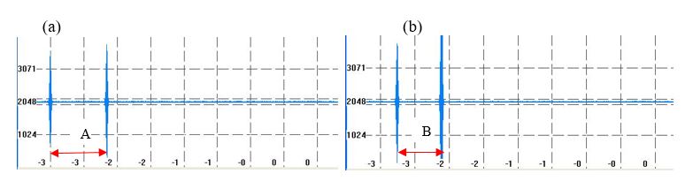
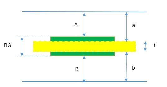
Dual probe measurement uses a block gauge to determine L=A+B+BG first, where A is the distance between reference mirror signal and top surface signal in top probe, B is the distance between reference mirror signal and bottom surface signal in bottom probe at the block gauge, and BG is the known thickness of metal block gauge. The typical signal at block gauge is in Figure 5. Then, the thickness of sample can be calculated from t=L-a-b, where a is the distance between reference mirror signal and top surface signal in top probe and b is the distance between reference mirror signal and bottom surface signal in bottom probe at the sample. Refer to Figure. 6. For dual probe measurement, one doesn’t need to know the refractive index beforehand.
Figure 4. A typical interference signal of the wafer for the top (a) and bottom (b) probe. a is a distance between the reference mirror signal and the top surface signal of the wafer. b is a distance between the reference mirror signal and the bottom surface signal of the sample.
Figure 5. A typical interference signal at block gauge for the top (A) and bottom (B) probe. A is a distance between the reference mirror signal and the top surface signal of the block gauge. B is a distance between the reference mirror signal and the bottom surface signal of the block gauge.
Figure 6.The procedure of the thickness measurement with dual probe is the following: first, it determines L=A+B+BG at the position of block gauge. Then, it measures sample thickness( t=L-a-b) at the sample position. The line square in the picture is block gauge of known thickness (500μm) and the dotted square is sample thickness.