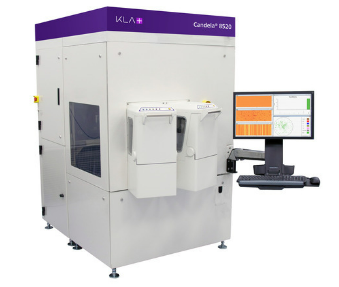
The Candela® 8520 2nd generation integrated surface and photoluminescence inspection system is designed for advanced characterization of substrate and epitaxial defects for the power device market and related applications. Implementation of automated wafer inspection with statistical process control (SPC) methodology can significantly cut yield loss due to epi defects, minimize metal-organic chemical vapor deposition (MOCVD) reactor process excursions, and increase MOCVD reactor uptime. The Candela 8520 is the successor to the Candela CS920, which was the first of its kind to integrate macro/micro detection for surface and crystal defects in a unified inspection platform. It employs proprietary optical technology to simultaneously measure scatter intensity at varying angles of incidence, topographic variations, surface reflectance, phase shift and photoluminescence for automatic detection and classification of a broad range of defects of interest (DOI).
Automated defect inspection for LED materials, enabling enhanced quality control of substrates, fast time-to-root cause determination, and improved MOCVD process control
A single-tool solution that combines multiple optical inspection techniques in a single scan for maximum efficiency in automated defect detection and classification
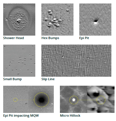
High sensitivity to yield-impacting defects across multiple compound semiconductor substrates
The 8520 system’s multiple detection channels enable understanding of process related issues and identification of yield-impacting defects. The inspection method achieves full-surface coverage in minutes with high-resolution images and wafer maps with automatically classified defects.