HMI eScan 1100
The first multiple e-beam (multibeam) wafer inspection system for in-line defect inspection applications. Following in the footsteps of the eScan 1000, the eScan 1100 offers new levels of efficiency in high throughput wafer inspection. Targeting the 3 nm node and beyond, the eScan 1100 is the first generation of systems in our multibeam roadmap to bring high-throughput, high-resolution e-beam inspection into volume manufacturing environments.
Key features & benefits
- Throughput:With 25 beams, the eScan 1100 will increase throughput by up to 15 times compared to single e-beam inspection tools, thanks to its multibeam technology, a high-speed wafer stage and advanced computational algorithms.
- Key technologies:Compared to the eScan 1000, the eScan 1100 includes an improved electron optics system capable of creating and controlling 25 primary electron beams with higher resolution, collecting and processing the resulting secondary electrons, minimizing beam-to-beam crosstalk, and delivering consistent imaging quality across all beams. It also features a high-speed stage to increase the system’s overall throughput and a high-speed computational architecture to process the streams of data from the multiple beamlets in real time. Advanced charging control (ACC) and high-voltage flooding technology provides comprehensive charging control capabilities to handle challenging voltage contrast inspection layers from Logic and Memory devices. Additionally, its proprietary die-to-database defect detection capability enables chipmakers to further enhance defect sensitivity and to monitor EUV mask defects using wafer print check. It is capable of detecting defects overlooked by optical inspection systems in a fraction of the time that it takes single e-beam solutions, enabling a broader adoption of multibeam inspection in high-volume manufacturing.
- Multimode operation: The eScan 1100 can be used for both voltage contrast defect inspection and physical defect inspection. This allows it to detect electrical defects (including open, short and leakage defects) and patterning defects down to 7 nm.
Applications
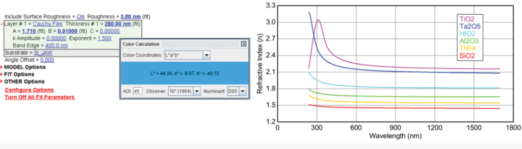
1. Optical Coatings
Characterize both thickness and refractive index for single- and multi-layer coatings; anti-reflection, high-reflection, or decorative coatings. Calculate the color coordinates for your coating stack under different lighting conditions.
2. Semiconductors
Traditional ellipsometry applications are still going strong. Characterize any semiconductor material: resists, photomasks, SiON, ONO stacks, low-k dielectrics, high-k gates, SOI, SiGe, II-VI and III-V ternary and quaternary compounds.
3. Chemistry/Biology
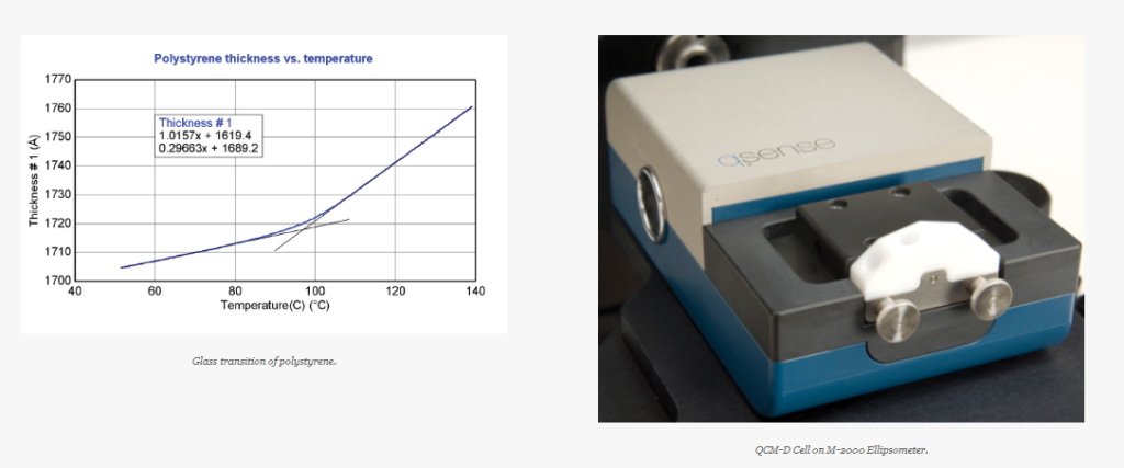
The M-2000 can be used for a variety of chemical and biological applications, either as a stand-alone tool or in combination with one of our many accessories. Study materials under liquid ambient, at high or low temperatures, or in conjunction with QCM-D measurements.
4. Conductive Organics
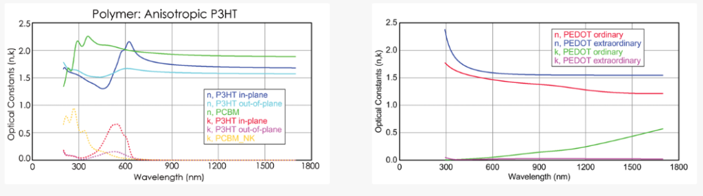
Great progress has occurred in the area of organic layers and stacks used for display (OLED) or photovoltaic applications. There are many different materials being studied, from small molecules such as Alq3 to conjugated polymers such as P3HT. Often multiple materials are blended together – which requires the wide spectral range of the M-2000 – to probe different wavelengths where the organics are optically different. Long-chain molecules may also have significant anisotropy, where orientational stacking of the polymer chains produces different optical constants in different directions.
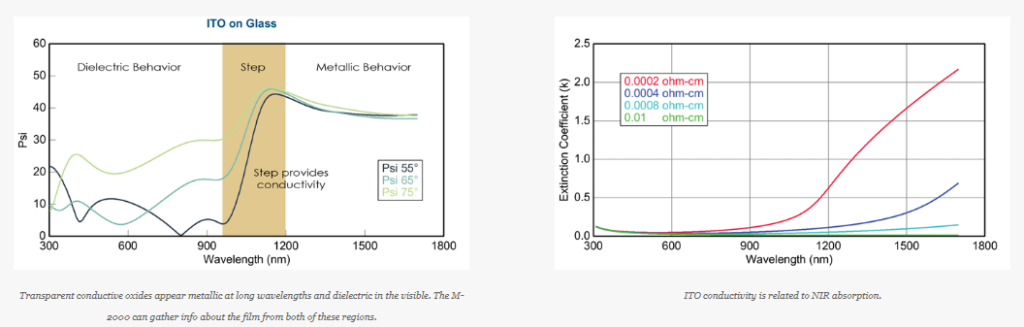
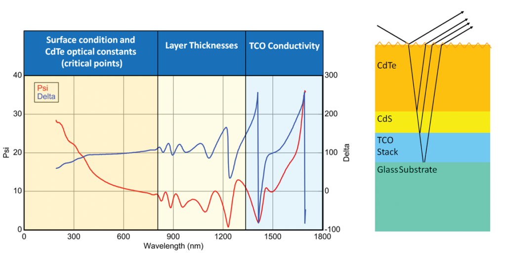
5. Photovoltaics
Film thickness and optical properties are critical to performance of solar devices. Ellipsometry is used for development and monitoring of all PV materials: a-Si, μc-Si, poly-Si, AR Coatings (SiNx, AlNx…), TCO Films (ITO, ZnOx, doped SnO2, AZO), CdS, CdTe, CIGS, organic PV materials, and dye sensitized films.